Every digital image your machine vision camera captures is built from pixels — tiny squares of light measurement arranged in a grid, each recording a single brightness value. At one level, this sounds simple. But the details of how pixels work, how many you need, and how pixel size relates to what your AI inspection system can detect form the foundation of every hardware specification decision in machine vision. If you are new to the field, this guide provides a clear, practical understanding of image pixels in machine vision — from what a pixel actually is to how to calculate the resolution your inspection application requires.
Key Takeaways
- A pixel is the smallest measurement unit in a digital image — each one records a single light intensity value from a defined physical area on the sensor.
- Resolution (megapixels) tells you how many pixels the sensor has in total; pixel size (in microns) indicates how sensitive each one is to light — these represent different trade-offs.
- For reliable defect detection in machine vision, the smallest defect must span at least 3–5 pixels in the image — this requirement drives your camera and lens selection from the start.
What Is a Pixel in Machine Vision?
The Basic Unit of a Digital Image
A pixel (short for “picture element”) is the smallest addressable unit in a digital image. In machine vision camera sensors, each pixel is a physical photodetector — a tiny square of silicon that converts incoming photons (light particles) into an electrical charge. The stronger the light, the higher the charge, and the brighter that pixel appears in the final image.
Every pixel records a single value: its brightness at the moment of exposure. On a monochrome (grayscale) sensor, that value ranges from 0 (pure black, no light) to 255 (pure white, maximum light) for an 8-bit sensor, or from 0 to 65,535 for a 16-bit sensor. On a color sensor, each pixel is covered by a color filter (red, green, or blue), and the camera uses a demosaicing algorithm to reconstruct full-color information by combining neighboring pixels. Most industrial machine vision applications for defect detection use monochrome sensors — providing higher effective resolution, better light sensitivity, and simpler processing.
How Pixels Form an Image
A camera sensor contains millions of these pixels, arranged in a rectangular grid. A 5-megapixel camera has approximately 5,000,000 pixels — arranged in a grid roughly 2,590 pixels wide by 1,944 pixels tall. When the camera captures an image, every pixel in that grid simultaneously records the light falling on it at that moment. The result is a 2D map of light intensity across the entire scene — the digital image.
In machine vision, this image is then processed by inspection software. In traditional rule-based systems, the software applies brightness thresholds or geometric measurements to the pixel grid. In AI-based inspection systems, a trained deep learning model analyzes pixel patterns across the entire image to detect, classify, and measure defects at pixel-level resolution.
Pixel Size vs. Resolution: Two Different Things
What Is Pixel Size?
Pixel size refers to the physical dimensions of each individual pixel on the camera sensor, measured in micrometers (µm). Common industrial camera pixel sizes range from 1.6 µm to 3.76 µm, with some specialized sensors going larger. Pixel size is a fixed property of the sensor design — you cannot change it through software settings.
Pixel size determines two critical performance characteristics:
- Light sensitivity: Larger pixels have a bigger photodetector area, collecting more photons per exposure. They produce less noise in low-light conditions — useful for dark-field inspection or fast-moving production lines where exposure time is short.
- Spatial resolution within a given sensor format: Smaller pixels allow more pixels to fit onto a sensor of the same physical size, increasing total resolution (megapixels) within the same sensor format.
A common rule in machine vision engineering is that pixel size should be approximately one-tenth of the required measurement tolerance. If you need to measure a dimension to ±0.1 mm accuracy, each pixel should represent approximately 0.01 mm (10 µm) or smaller in object space. For defect detection, rather than measurement, the 3–5 pixels per feature rule is the industry standard.
What Is Resolution?
Resolution — typically expressed in megapixels — is the total number of pixels on the sensor. A 5 MP camera has approximately 5 million pixels. Resolution determines the maximum spatial detail the camera can capture across its entire field of view, and it is the primary factor engineers adjust when they need to detect smaller features across the same inspection area.
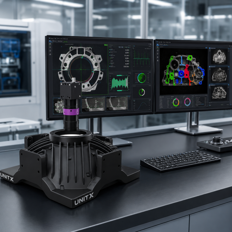
High-resolution cameras can detect surface anomalies as small as 1.5 micrometers in precision applications. The CorteX AI visual inspection system supports single-image capture up to 50 MP — enabling 0.02 mm/pixel resolution across a 100 mm wide field of view, sufficient to detect sub-pixel defects using deep learning sub-pixel inference techniques.
The Key Misconception: More Megapixels Is Not Always Better
Beginners often assume that higher resolution always produces better inspection results. In practice, this is not always true. Higher-resolution cameras:
- Generate larger image files, requiring more computing power and data bandwidth
- Reduce achievable frame rates — a 50 MP camera running at 30 fps generates 50× more data per second than a 1 MP camera at the same frame rate
- Often use smaller pixels to fit more onto the same sensor format, reducing per-pixel light sensitivity
- Require higher-quality lenses to resolve finer detail (a lens that performs well at 5 MP may not resolve 20 MP effectively)
The right resolution is the minimum required to meet your detection requirement — not the maximum available. Over-specifying resolution increases cost, adds system complexity, and may slow inspection speed below what the production line cycle time allows.
How to Calculate the Resolution You Need
The Object Space Resolution Formula
Object space resolution — the physical size each pixel represents on the part being inspected — connects everything together:
Object Space Resolution (mm/pixel) = Field of View (mm) / Number of Pixels
And the inverse, to determine the minimum camera resolution required for a given inspection task:
Required Pixels = Field of View (mm) / Minimum Detectable Feature (mm) × Pixels-Per-Feature Safety Factor
Worked Example: Surface Scratch Inspection
An inspection system needs to detect scratches as narrow as 0.2 mm on a 50 mm × 50 mm component face. Using a 3-pixel-per-feature minimum:
- Required object space resolution: 0.2 mm / 3 = 0.067 mm/pixel
- Required horizontal pixel count: 50 mm / 0.067 mm/pixel = 746 pixels
- Required vertical pixel count: 50 mm / 0.067 mm/pixel = 746 pixels
- Total required resolution: 746 × 746 = approximately 0.56 MP
A 1.3 MP camera (1,280 × 1,024 pixels) provides a comfortable margin. For a 5× safety factor, a 5 MP camera would be appropriate. This calculation framework applies universally — the inputs change per application, but the core logic is consistent.
| Camera Resolution | Pixel Grid | Min Feature (50mm FOV) | Typical Application |
| 1.3 MP | 1,280 × 1,024 | 0.12 mm | General inspection, barcode |
| 5 MP | 2,592 × 1,944 | 0.058 mm | Surface defect, scratch detection |
| 12 MP | 4,096 × 3,000 | 0.037 mm | Fine surface, PCB inspection |
| 25 MP | 5,120 × 4,800 | 0.029 mm | Semiconductor, micro-defect |
| 50 MP | 8,192 × 6,144 | 0.018 mm | Large part + micro-defect, EV battery |
Note: Min Feature column assumes 3-pixel-per-feature criterion at 50 mm H-FOV.
How Pixels Enable AI Defect Detection
From Pixel Grid to Defect Classification
A traditional rule-based vision system works directly with pixel values: “if pixel brightness in zone X is below threshold Y, flag a defect.” This approach is rigid — it cannot handle natural variation in surface texture, lighting inconsistency, or defect morphology that differs from the predefined pattern.
An AI visual inspection system uses the full pixel grid as input to a deep learning model. The model — typically a fully convolutional network or similar architecture — processes the entire pixel map simultaneously, identifying spatial patterns across groups of pixels that correspond to specific defect types. It is trained on examples of defective and non-defective parts, allowing it to learn the visual patterns of real defects in context, rather than relying on fixed pixel threshold rules.
The output of AI inference on a pixel grid is not just a pass/fail signal — it can be a segmentation map where every pixel is classified as “good material,” “scratch,” “dent,” or other categories. This pixel-level deep learning segmentation allows engineers to measure defect area in mm², characterize defect boundary shape, and distinguish functional defects from cosmetic variation. Exploring how CorteX processes pixel data at up to 100 MP/s inference speed illustrates how this works in a production environment.
![]()
From pixel to defect detection: higher pixel density means each square millimeter of the inspected part is represented by more pixels — the foundation of why resolution selection starts with the smallest defect you need to detect, not the largest camera you can buy.
Pixel Size, Sensor Format, and the Lens Connection
Why Lens and Sensor Must Be Matched
A high-resolution sensor only delivers its rated pixel count if the lens can actually resolve that level of detail. Every lens has a resolving power — expressed as line pairs per millimeter (lp/mm) — that describes the finest detail it can project sharply onto the sensor. If a 20 MP sensor requires resolving 150 lp/mm but the lens is only rated for 80 lp/mm, the final image will be blurred at finer detail levels, effectively wasting half the sensor’s resolution.
The sensor format must also match the lens image circle. A lens designed for a 1/2″ sensor cannot properly cover a 2/3″ sensor without vignetting (darkening) at the edges. This means some pixels near the image corners will receive less light and produce lower-quality readings. Matching sensor format, pixel size, and lens specification is a three-way constraint that determines the actual achievable resolution in a real industrial system.
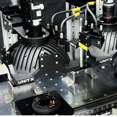
If you are specifying an AI visual inspection system and want to understand the pixel resolution requirements for your specific parts and defect types, contact the UnitX team for an application-specific optical system analysis.
Frequently Asked Questions
What is a pixel in machine vision?
A pixel is the smallest individual element on a camera sensor — a single photodetector that measures the brightness of light falling on a tiny area during image capture. The full grid of pixels on the sensor forms the digital image. In machine vision, each pixel represents a physical measurement: the brightness of a specific point on the inspected part. More pixels mean finer spatial resolution and the ability to detect smaller features.
How many pixels do I need to detect a defect?
The standard guideline is that the smallest defect you need to detect should span at least 3 pixels in the image — and 5 pixels for reliable AI classification. If the minimum defect is 0.1 mm and each pixel represents 0.033 mm (object space resolution), a 0.1 mm defect spans 3 pixels. Required resolution can be calculated as: (Field of View in mm) / (minimum defect size / pixel-per-feature requirement).
What is the difference between pixel size and camera resolution?
Pixel size is the physical dimension of each individual photodetector on the sensor, measured in micrometers (e.g., 3.45 µm). Resolution (megapixels) is the total number of pixels on the sensor. A large sensor with small pixels can provide both high sensitivity (from total sensor area) and high resolution (from pixel count). Pixel size primarily affects light sensitivity; total resolution determines how much spatial detail the camera captures.
Why does pixel size affect image quality in industrial inspection?
Larger pixels collect more photons during the same exposure time, producing lower-noise images — critical in fast-moving production lines where exposure time must be short to avoid motion blur. Smaller pixels pack more resolution into the same sensor format but are less sensitive to light, requiring brighter illumination or longer exposure times. In dark-field illumination setups, where light levels are inherently low, cameras with larger pixels often outperform high-resolution cameras with very small pixels in real inspection conditions.
What camera resolution does UnitX’s AI inspection system support?
UnitX’s CorteX AI visual inspection system supports single-image capture up to 50 MP, combined with inference processing at up to 100 MP/s. This means a 50 MP image can be processed in approximately 0.5 seconds — fast enough for high-volume production inspection. The OptiX imaging system pairs with CorteX to deliver this resolution across fields of view up to 500 mm wide, enabling large-part inspection (e.g., automotive body panels, battery modules) at defect-level pixel density. Learn more about the FleX full-system platform that integrates OptiX and CorteX in a turnkey AI visual inspection solution.