Semiconductor packaging has entered an era of unprecedented complexity. Advanced formats, including flip-chip BGA, fan-out wafer-level packaging, and 2.5D chiplet integration, have introduced defect modes that require sub-pixel detection accuracy across dozens of inspection points. The global advanced packaging market reached $45.13 billion in 2025 and is projected to grow to $94.33 billion by 2034, driven by AI compute demand. Every yield point matters: analysts estimate that a 1% improvement in semiconductor yield can generate roughly $150 million in additional profit per facility. Yet, on most packaging lines today, inspection is still handled by rule-based systems that were not designed for variable defect geometries or high-mix production.
UnitX has deployed AI visual inspection across semiconductor packaging lines for OSATs and IDMs tackling exactly these challenges. This guide documents the deployment steps our teams follow, from initial site assessment to full MES integration, the imaging trade-offs that matter most for packaging substrates, and the three mistakes that can delay SAT by weeks.
Key Takeaways
- A structured 5-stage framework can take a semiconductor packaging line from assessment to production SAT in 7 days, compared to 6 or more weeks for rule-based optical inspection.
- Software-defined lighting is not optional in packaging. Solder ball, underfill, and substrate surface variations demand lighting adaptability that fixed-angle illumination cannot deliver.
- Sample-efficient AI helps solve the labeling bottleneck: 5 defect images per category are sufficient for CorteX, while FleX-Gen reduces that requirement to as few as 3 real samples by generating synthetic training data.
- MES integration closes the quality loop. Without it, defect data remains within the inspection station and cannot drive upstream process correction.
Why Semiconductor Packaging Inspection Has Hit a Wall
The Defect Landscape in Advanced Packaging
Back-end semiconductor packaging introduces a class of defects that front-end wafer inspection does not encounter. Flip-chip bumping can produce voids, incomplete solder joints, missing bumps, and coplanarity failures. Die attach processes introduce delamination, die tilt, and adhesive squeeze-out. Final package inspection must detect mold voids, wire sweep, solder ball placement issues, and package warpage. As IEEE Spectrum reports, the shift toward 3D architectures and advanced packaging formats has fundamentally changed the nature of the defects that inspection systems must identify. Many of these failure modes remain invisible to traditional optical systems unless the lighting is precisely matched to the surface geometry.
Packaging lines are also high-mix environments. A single OSAT line may handle dozens of package types within a single shift. Rule-based inspection requires a separate recipe for each package type, and each recipe must be programmed, calibrated, and validated by an engineer. The programming overhead alone can consume weeks for every new product introduction.
Why Rule-Based Optical Inspection Fails for BGA and Flip Chip
Rule-based machine vision relies on fixed thresholds applied to pixel brightness, edge contrast, or geometric measurements. It works reliably when defects are deterministic in size, shape, and position. Advanced packaging defects are none of those things. A void in underfill can appear in any location and at any size. A missing bump in a flip-chip array may be a single ball among thousands. A warped package may shift the entire image outside the measurement window.
The result is a high false rejection (FR) rate that causes manual review queues to grow. Quality engineers spend hours reviewing images that were incorrectly flagged. Meanwhile, actual defects, especially those with subtle contrast variations or unexpected morphology, can escape to downstream testing or even reach the customer. According to research published in MDPI Engineering Proceedings, traditional inspection methods are no longer adequate for modern high-precision, high-efficiency semiconductor production demands.
When combined with data on the growth of advanced packaging inspection equipment, a clear pattern emerges: the semiconductor inspection tools market is expanding because existing rule-based systems cannot scale to the defect complexity introduced by chiplets, fan-out packaging, and 2.5D integration. For packaging engineers, the implication is clear: AI machine vision is no longer a future upgrade. It is a present-day necessity for any production line running high-volume flip-chip or BGA packages.
The 5-Stage AI Inspection Deployment Framework
We have validated the following deployment sequence across semiconductor packaging customers. The goal is a production-ready system with Site Acceptance Testing (SAT) completed within 7 days. Each stage has a defined deliverable and a quality gate before the next stage begins.
Stage 1: Inspection Point Mapping (Day 1)
Before any hardware is installed, map every checkpoint in the packaging process where a defect could escape if left uninspected. For a typical flip-chip line, this includes incoming die inspection, bumping or underfill inspection, die attach inspection, wire bond or flip-chip attach, encapsulation, singulation, and final package testing. For each checkpoint, document the defect types of concern, the part throughput rate, the available space for camera mounting, and the MES trigger signal available from the PLC. This map becomes the single source of truth for imaging configuration and model scope in Stages 2 and 3.
We recommend prioritizing checkpoints based on defect cost. A defect caught during bumping may cost only a few cents to rework. The same defect reaching final test or resulting in a field return may cost hundreds of dollars in die loss, rework, and customer disposition. Prioritize inspection points where defect escape creates the highest downstream cost.
Stage 2: Imaging and Software-Defined Lighting Configuration (Day 2)
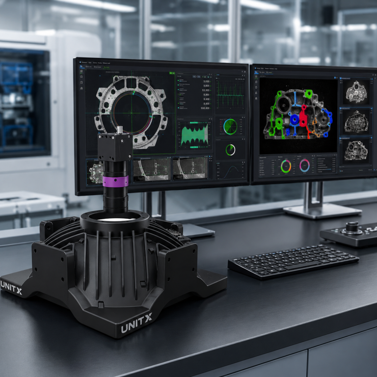
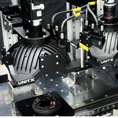
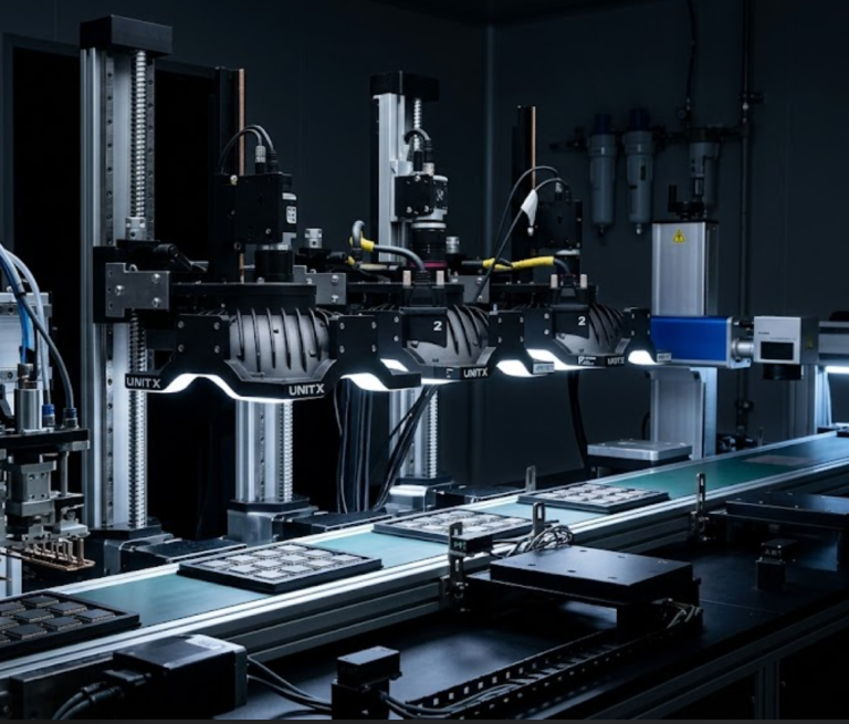
Semiconductor packaging substrates present some of the most challenging imaging conditions in manufacturing: highly reflective solder balls, low-contrast underfill boundaries, fine-pitch bump arrays, and translucent mold compounds. The UnitX AI visual inspection platform addresses these challenges through OptiX, a 32-channel software-defined lighting and multi-angle imaging system that cycles through 50 lighting modes per second.
For BGA and flip-chip inspection, we configure OptiX to capture both brightfield and darkfield illumination passes in a single fly-by capture at a line speed of 1 m/s. The brightfield pass reveals solder ball presence, shape, and coplanarity. The darkfield pass reveals surface contamination, micro-cracks, and underfill voids that disappear under direct illumination. Both images sets are passed simultaneously to CorteX for multi-channel inference without slowing the line. The standard 50 × 100 mm field of view covers most package formats, while the modular OptiX configuration enables coverage of larger die arrays through multi-head setups.
Stage 3: Sample-Efficient Model Training (Days 3-4)
The labeling bottleneck delays more AI inspection deployments than any other technical issue. Traditional deep learning approaches typically require 500 to 5,000 labeled images per defect category. On a packaging line running at high yield, collecting that many defect samples can take months. The CorteX AI visual inspection system was designed to eliminate this constraint.
CorteX trains effective models using as few as 5 labeled images per defect category. For categories where even 5 samples are difficult to collect, FleX-Gen generates synthetic defect variants from just 3 real samples, expanding the training set without additional line time. The full model training cycle runs in approximately 30 minutes. Once training is complete, quality engineers validate the model against a holdout set of known-good and known-defect images before the system advances to Stage 4.
NVIDIA’s technical research confirms that fine-tuning AI models on domain-specific semiconductor images can push defect classification accuracy to 98.51%. Result that previously took months to achieve with general-purpose models are now achievable in days using sample-efficient approaches.
Stage 4: Edge Deployment and PLC Integration (Days 4-5)
CorteX performs inference at 100 MP/s on edge hardware installed directly at the inspection station, with zero dependency on cloud connectivity. Sub-50 ms latency from image capture to reject signal is achievable at packaging throughput rates of up to 1,200 parts per minute. Research on machine vision and PLC integration for Industry 4.0 confirms that real-time synchronization between the vision system and the PLC is the key factor determining whether AI inspection performs consistently across all shifts.
During Stage 4, we configure three integration points. First, PLC trigger signals instruct OptiX when to capture images, timed precisely to the part position on the conveyor or index table. Second, the reject mechanism receives the AI pass or fail signal within the part’s dwell time, activating the diverter before the part advances. Third, the edge system logs every inspection result, including the raw image, AI confidence score, and final decision, to a local data store that feeds the MES in Stage 5. We verify timing accuracy through a 200-part test run before advancing.
Stage 5: MES Integration and Closed-Loop Quality Control (Days 6-7)
An AI inspection system that cannot share data with the factory’s Manufacturing Execution System (MES) operates in isolation. Defect data that remains trapped within the inspection station cannot trigger upstream process corrections, feed SPC charts for quality engineers, or provide the regulatory traceability that OSAT customers require.
UnitX integrates directly with customer MES platforms through standard industrial protocols, enabling real-time data traceability and closed-loop quality control. Defect counts and categories, image thumbnails, and inspection timestamps are written to the MES during every cycle. When defect frequency for a specific package type exceeds a control limit, the MES can alert process engineers or automatically trigger a hold on the upstream process that produced the affected lot. This closes the quality loop that rule-based systems leave open.
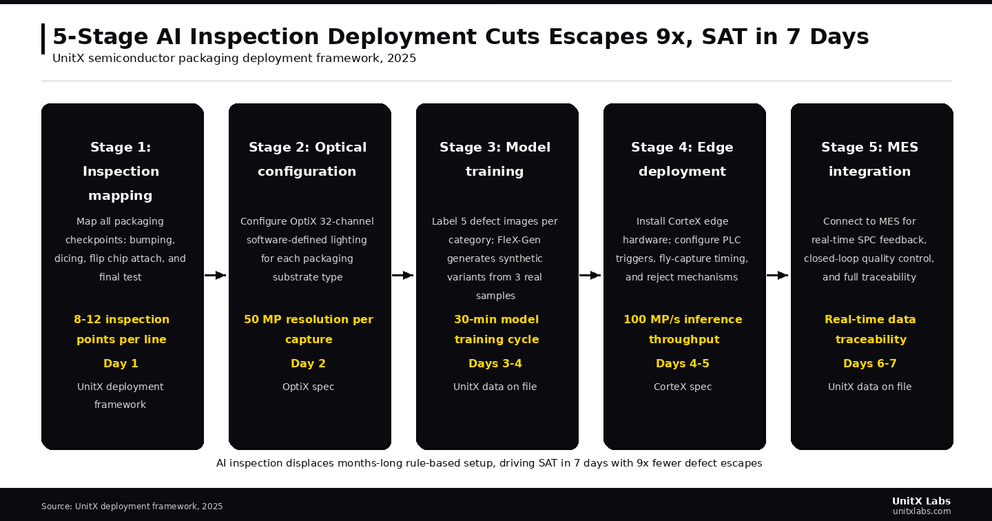
AI inspection replaces months-long rule-based setup processes, enabling SAT completion in 7 days while reducing defect escapes by up to 9x.
Three Mistakes That Stall Semiconductor Packaging Inspection Deployments
Mistake 1: Scoping Inspection to One Process Step
Teams that deploy AI inspection only at the final package inspection stage catch defects too late, after the most expensive process steps have already been completed. A deployment that covers bumping, die attach, and final inspection in parallel catches defects at their cheapest intervention point and generates process feedback that improves upstream yield. We recommend scoping inspection coverage across the full packaging flow from day one.
Mistake 2: Underspecifying the Lighting Configuration for the Substrate Type
Packaging teams that adapt camera settings from wafer inspection configurations often find that solder ball inspection produces high false rejection rates. BGA and flip-chip substrates require dedicated lighting profiles. Software-defined lighting with independent channel control, rather than fixed illumination, is the correct starting point for any packaging inspection application.
Mistake 3: Delaying MES Integration to a Second Phase
MES integration is consistently deprioritized during initial deployment and just as consistently identified as a missed opportunity during deployment retrospectives. The data generated during the first weeks of AI inspection in production is often the most valuable data the system will ever produce because it captures the baseline defect state before any process corrections are made. Integrating MES from day one preserves that data.
Infosys’s analysis of semiconductor yield improvement highlights end-to-end digitization as the primary driver of sustained yield gains. MES integration serves as the bridge between AI inspection and continuous improvement. IEEE’s review of AI in semiconductor manufacturing similarly notes that closed-loop AI systems, rather than isolated point-tool deployments, are driving the most significant quality gains at leading fabs.
Frequently Asked Questions
How many defect samples are needed to train an AI inspection model for a new package type?
CorteX requires 5 labeled defect images per category to train an effective model. FleX-Gen can reduce this requirement to as few as 3 real samples by generating synthetic variants. This is 100x to 1,000x fewer samples than traditional deep learning approaches require, which is critical in packaging environments where defect samples are rare on well-controlled lines.
Can AI inspection run at flip-chip production speeds without stopping the line?
Yes. The OptiX fly-capture capability operates at speeds of up to 1 m/s without requiring part stops or introducing motion blur. CorteX completes inference in under 50 ms, well within the dwell time available at typical flip-chip attach and BGA placement throughput rates. The reject signal reaches the PLC before the next part enters the inspection zone.
What happens to existing inspection equipment when AI inspection is deployed?
Most deployments augment rather than immediately replace legacy rule-based systems. During SAT, we run both systems in parallel, comparing false acceptance (FA) and false rejection (FR) rates before switching primary control to the AI system. UnitX case studies document deployments in which legacy inspection equipment remained in a monitoring role after AI inspection assumed primary control, providing an additional safety layer during the confidence-building period.