Semiconductor packaging is among the most technically demanding inspection environments in manufacturing. As packaging architectures evolve from traditional wire-bonded packages to flip-chip, 2.5D interposers, and panel-level packaging, the defect taxonomy expands and tolerance windows tighten. A solder bump height deviation of just a few microns can create an open circuit; a subsurface void in the underfill material can initiate delamination under thermal cycling.
According to a 2025 manufacturing AI analysis, 72% of manufacturers have adopted AI vision for inspection. Yet semiconductor packaging remains one of the most complex verticals for deployment, as inspection requirements span multiple defect classes, modalities, and sub-micron geometric precision. This guide covers the defect taxonomy for semiconductor packaging inspection, maps inspection techniques to defect types, and outlines a five-week deployment roadmap validated across production environments.
Key Takeaways
- Semiconductor packaging produces 8+ distinct defect categories across wire bonding, flip-chip, BGA, encapsulation, and substrate processes — each requiring matched imaging and AI configuration.
- Optical AI inspection handles surface and near-surface defects at production line speed; subsurface void detection and internal delamination require complementary modalities such as X-ray or acoustic inspection.
- Software-defined 2.5D imaging captures both surface defects and shallow depth variation (e.g., bump coplanarity, die tilt) in a single scan, reducing the number of inspection stations required per line.
- The rarest packaging defects are often the most consequential. Sample-efficient AI, capable of training from 5 labeled images per category, with FleX-Gen reducing this to 3 real samples, makes rare-defect models deployable in days rather than months.
- 5-day site acceptance testing is achievable for standard packaging inspection applications, compared to the 3–6 month pilot periods typical of complex semiconductor deployments using conventional inspection platforms.
- PLC-level integration and real-time MES traceability are required for semiconductor packaging inspection to meet the documentation standards of semiconductor supply chain customers.
The Semiconductor Packaging Defect Taxonomy
Surface and Near-Surface Defects (Optical AI Inspection)
The majority of semiconductor packaging defects are surface-accessible and detectable by optical AI inspection at production speeds. A technical review of semiconductor bonding inspection identifies the primary surface defect categories: solder voids (air pockets within solder joints that reduce contact area and cause hot spots), bridging between adjacent interconnects (unintentional electrical shorts), non-wet opens (solder failing to bond with the pad due to contamination or insufficient heat), wire sweep (displacement of wire bonds during plastic molding), and “golf ball” defects (misshapen solder balls).
For wire-bonded packages, AI inspection also detects broken or missing wires, incorrect wire routing, and bond wire contamination. Each of these defect types presents a distinct visual signature that requires matched illumination geometry — coaxial illumination for solder pad surface inspection, dark-field for scratch and contamination detection, and structured light for bump height and coplanarity measurement.
Subsurface Defects (Complementary Inspection Modalities)
Internal voids, delamination, and underfill distribution cannot be detected through optical inspection alone. As the INCURE semiconductor packaging QC framework documents, voids in bonding materials are particularly critical: they reduce effective thermal contact area and, under mechanical stress or thermal cycling, can act as crack initiation sites that lead to total bond failure.
Scanning Acoustic Microscopy (SAM) detects internal voids and delamination using high-frequency ultrasound. Automated X-Ray Inspection (AXI) penetrates silicon and molding compounds to reveal solder joint internal structure. For 2.5D and 3D packaging architectures — where inspection targets include TSVs, micro-bumps, and multi-layer interconnects — 3D X-ray CT reconstruction provides the volumetric view required to characterize defects at each packaging level.
AI inspection complements, rather than replaces, these modalities. Optical AI handles surface defects at production-line throughput (100% inspection), while X-ray and acoustic methods are typically used for sampling inspection or for high-value components where subsurface defect risk justifies the cycle time cost.
Inspection Technique Selection for Semiconductor Packaging
| Defect Type | Inspection Method | Illumination / Modality | In-Line Suitable? |
| Bump coplanarity / height | Optical AI (2.5D) | Structured light | Yes |
| Solder bridging / shorts | Optical AI | Coaxial / multi-angle LED | Yes |
| Wire bond defects | Optical AI | High-magnification darkfield | Yes |
| Surface contamination / particles | Optical AI | Darkfield oblique | Yes |
| Solder void (internal) | X-ray AXI | 2D or 3D X-ray | Sampling only |
| Underfill delamination | Acoustic (SAM) | Ultrasound | Sampling only |
The advancement toward 2.5D and 3D advanced packaging is also advancing glass substrate adoption. Toray Engineering’s 2025 launch of an inspection system for large glass substrates — the industry’s first to support double-sided and internal defect inspection for glass core interposers and rewiring carriers used in panel-level packaging — illustrates how the inspection technology frontier is extending to match the packaging technology frontier. For standard packaging inspection applications, optical AI combined with software-defined illumination covers the majority of in-line inspection requirements today.
Deploying AI Inspection in Semiconductor Packaging: 5-Week Roadmap
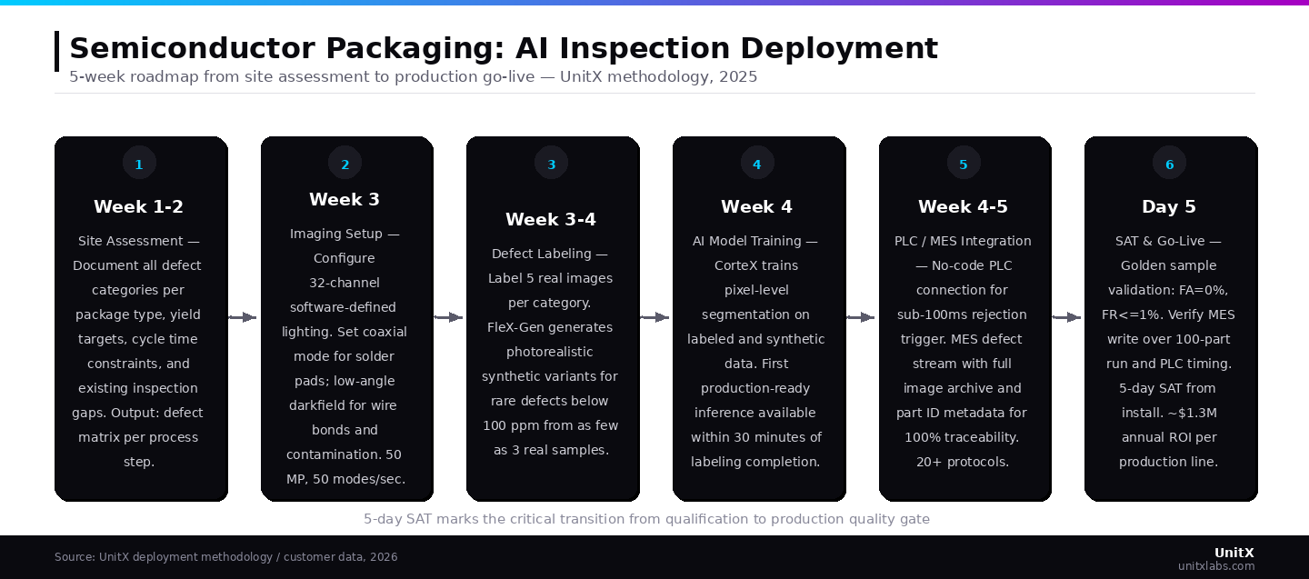
A 5-day SAT marks the critical transition from qualification to a production quality gate — the key milestone in achieving a 12-month payback
Week 1–2: Site Assessment and Defect Profile Documentation
The most common cause of extended semiconductor packaging inspection deployments is insufficient pre-deployment characterization of the defect profile. Before any equipment is installed, the quality engineering team should document: all defect categories by package type and process step, the occurrence rate for each category (parts per million), the minimum detectable feature size for each defect type, existing inspection coverage and identified gaps, and the cycle time budget available for the new inspection station.
According to the 2025 Visual AI in Manufacturing landscape, integration complexity and model explainability remain the top deployment challenges in semiconductor environments — both of which can be mitigated through a thorough site assessment that scopes integration requirements before equipment selection. The output of this phase is a defect matrix linking each defect type to its required imaging modality, minimum detection sensitivity, and cycle time constraint.
Week 3: Imaging Architecture Configuration
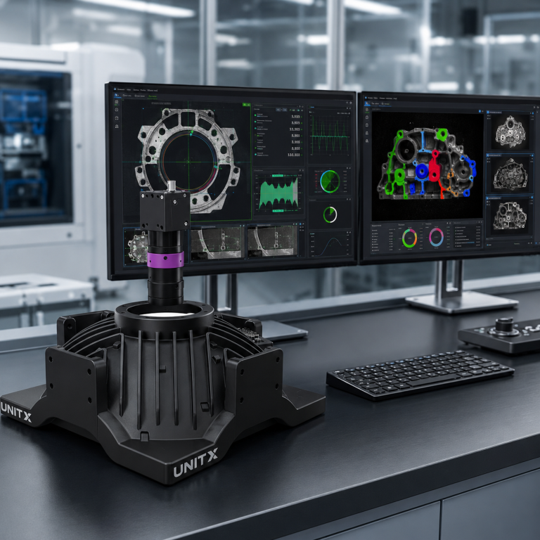
Semiconductor packaging inspection typically requires multi-mode imaging within a single station: coaxial illumination for solder pad surface inspection, structured light for bump height and coplanarity measurement, and dark-field for contamination and wire bond defect detection.
The OptiX software-defined imaging system addresses this through 32-channel, independently controllable LED arrays that cycle through 50 lighting modes per second — enabling coaxial, dark-field, and structured light patterns within a single capture sequence without mechanical reconfiguration. The 2.5D imaging mode captures both surface defect information and shallow depth profiles (e.g., bump height, die tilt, pad coplanarity) using a single CMOS area scan camera, with 3D reconstruction rates of 6 per second at 5 MP resolution. For high-density packaging applications with fine-pitch features, the system’s 50 MP imaging resolution and 3 μm Z-axis repeatability provide the sub-pixel precision required to characterize bump-to-bump dimensional variation.
Weeks 3–4: Defect Labeling and Model Preparation
Rare packaging defect categories — such as head-in-pillow joints, lifted ball bonds, and incomplete encapsulation — may occur at rates below 100 parts per million. Collecting 500 real examples of each to train conventional deep learning models requires months of production data accumulation before deployment can begin.
A sample-efficient approach eliminates this bottleneck. The CorteX AI system trains effective pixel-level segmentation models from as few as 5 labeled images per defect category. FleX-Gen’s synthetic defect generation reduces this requirement to as few as 3 real images per category for applications where defect morphology is consistent enough for augmentation. According to UnitX production deployment data, this approach accelerates model deployment by up to 3X compared to conventional AI inspection platforms, enabling the 7-day site acceptance testing timeline required to minimize production downtime during inspection system qualification.
Week 4–5: PLC and MES Integration
Semiconductor packaging supply chains require 100% part traceability — every component must be traceable to the specific inspection result, production batch, and wafer lot from which it came. This places demands on the MES integration that exceed typical manufacturing inspection requirements: the inspection system must write defect classification data, images, and part identifiers to the MES within the production cycle time for every part, without exception.
Integration architecture is critical. Direct PLC-level integration with the AI inference system achieves sub-100ms detection-to-data-write latency, ensuring that even at 1,200 parts per hour, no part completes its inspection cycle before its data is recorded in the traceability system. UnitX supports 20+ industrial protocols for no-code PLC integration, along with an open SDK for MES data exchange — reducing the engineering effort that typically extends semiconductor inspection deployments.
Day 5 from Installation: Site Acceptance Testing (SAT)
The SAT protocol for semiconductor packaging inspection should include: verification that FA = 0% on the full golden sample set (zero defect escapes), FR ≤ 1% on clean parts (acceptable overkill rate), cycle time validation at full production speed, MES data write verification over a continuous 100-part run, and PLC rejection trigger timing validation.
Systems that achieve these criteria within 5 days of installation are considered production-ready. UnitX automotive and semiconductor packaging deployments typically achieve SAT within this window (UnitX customer data, 2026), producing an approximate $1.3M annual ROI per production line through combined defect escape reduction, scrap rate improvement, and inspection labor reallocation.
Common Deployment Pitfalls in Semiconductor Packaging Inspection
The most frequent deployment issue is a mismatched imaging configuration for the package geometry. For example, a coaxial-only setup deployed on a package with fine-pitch wire bonds will miss wire defects that require dark-field illumination to resolve. The second most common issue is under-scoped MES integration: teams plan for defect pass/fail data but discover mid-deployment that the customer’s quality system requires full defect image archives and positional coordinate data.
Scoping MES data requirements before deployment begins — specifically, the expected data format and per-part data transfer latency budget — prevents costly extensions to the integration timeline. Explore UnitX semiconductor inspection application coverage and customer case studies for documented deployment timelines across advanced packaging applications. To discuss deployment requirements for your specific package type, connect with a UnitX expert.
Frequently Asked Questions
Can a single AI inspection system handle multiple package types on the same line?
Yes, with software-defined illumination and a sample-efficient AI platform capable of maintaining multiple active model configurations. The key consideration is that each package type requires its own trained defect model — a QFN model is not transferable to a BGA package model without retraining, as defect geometry and acceptable appearance standards differ.
Systems with software-defined lighting handle the imaging reconfiguration automatically when the recipe changes, while sample-efficient AI enables rapid model addition as new package types are introduced without months of data collection.
How do you handle very high-density packaging (sub-50-micron bump pitch)?
Sub-50-micron bump pitch inspection requires higher magnification optics, closer working distance, and imaging resolution that may exceed standard 50 MP area scan cameras without optical magnification. For advanced packaging at or below 25-micron pitch, dedicated close-up inspection stations with higher numerical aperture (NA) optics and specialized illumination are typically required.
This is a specification discussion for pre-deployment site assessment — minimum detectable feature size and pitch requirements for the specific package design should be documented before imaging architecture is specified.
What is the difference between 2D and 2.5D inspection for semiconductor packaging?
Standard 2D imaging captures a flat image of the package surface — effective for detecting solder bridging, missing wire bonds, and contamination, but cannot measure bump height, die tilt, or depth-related geometry.
2.5D imaging adds shallow depth profiling using structured light techniques, enabling bump coplanarity measurement, die attach tilt detection, and surface profile characterization — all from a single CMOS sensor without requiring separate profilometry hardware. For advanced packaging applications where bump height variation impacts yield, 2.5D imaging provides the dimensional measurement capability that 2D-only systems cannot deliver, without the cycle time cost of full 3D CT scanning.