The AI visual inspection market is growing at a CAGR of nearly 20% and is projected to exceed $89 billion by 2033. Yet most manufacturers report that choosing the wrong system can be as costly as deploying no system at all. Vendor demos often look identical, and RFQ responses frequently cite 99% accuracy. The differentiating questions are rarely asked until month six of a failed deployment, when it becomes clear that the system cannot retrain on new defect types without months of engineering support, or that the imaging architecture cannot resolve the 0.05mm scratches your line produces most often.
This guide is built around five evaluation criteria that experienced quality engineers use to filter vendors before the demo stage — and five red flags that signal a system will underperform in your specific environment.
Key Takeaways
- Define your defect profile before speaking with vendors. Occurrence rate, visual complexity, and part geometry determine which system architectures are viable for your application.
- Lighting is not an afterthought. Software-defined, multi-angle lighting is the single largest determinant of whether a system can resolve subtle surface defects under variable production conditions.
- Sample efficiency equals deployment speed. A system that trains on 5 labeled images per defect category can be production-ready in 7 days; one requiring 500 images may take months.
- MES and PLC integration are not optional. Without closed-loop integration, AI inspection provides detection data but cannot trigger real-time quality interventions.
- A strong ROI benchmark is approximately $1.3M in annual ROI per production line for typical high-variation inspection deployments (UnitX customer data, 2026) — systems with 12-month payback periods are achievable in most automotive and battery applications.
- Manual inspection averages about 80% detection accuracy at best (Sandia National Laboratories, 2018) — with an additional 20–30% degradation after just one hour of continuous monitoring.
Step 1: Define Your Defect Profile Before Talking to Vendors
What a Defect Profile Actually Includes
Most buyers begin vendor conversations with statements like “we have surface scratches” or “we need to detect solder joint defects.” This level of specificity is insufficient for evaluating imaging architecture or AI model requirements.
A complete defect profile contains: the defect category (surface, dimensional, structural, cosmetic, process, or coating), typical occurrence rate per production volume, minimum detectable feature size (in microns), whether the defect varies in shape across production batches, and whether the part surface has texture or reflectivity that complicates imaging.
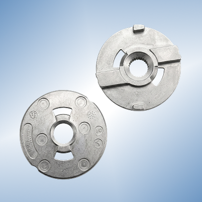
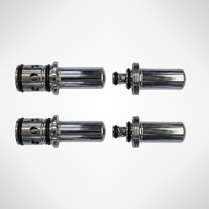
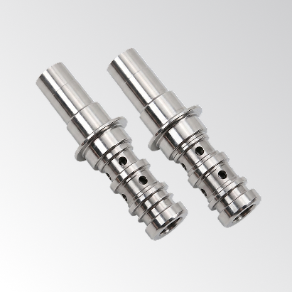
A battery tab laser weld defect is not the same inspection problem as a connector pin bent-angle deviation, even if both appear as “surface anomalies.” The battery inspection application requires high-speed defect detection on reflective metallic surfaces with consistent defect morphology, while connector pin inspection requires sub-pixel dimensional measurement across thousands of pin variants.
Occurrence Rate Drives Your Synthetic Data Strategy
If a specific defect type occurs fewer than 10 times per 10,000 cycles, waiting for real defect data to accumulate before training your AI model is not a viable strategy. This is where sample-efficient AI and synthetic defect generation become non-negotiable evaluation criteria rather than optional features. According to DataSpan’s 2025 manufacturing AI analysis, 72% of manufacturers have adopted AI vision for inspection — yet many underestimate how rare-defect occurrence rates drive their timeline to go live.
Step 2: Evaluate Imaging Architecture — The Variable Nobody Budgets For
Why Lighting Is the Most Underestimated Variable
Camera resolution and sensor megapixels are the specs manufacturers compare in RFQs. Lighting architecture is what actually determines whether a system can detect the defects that matter.
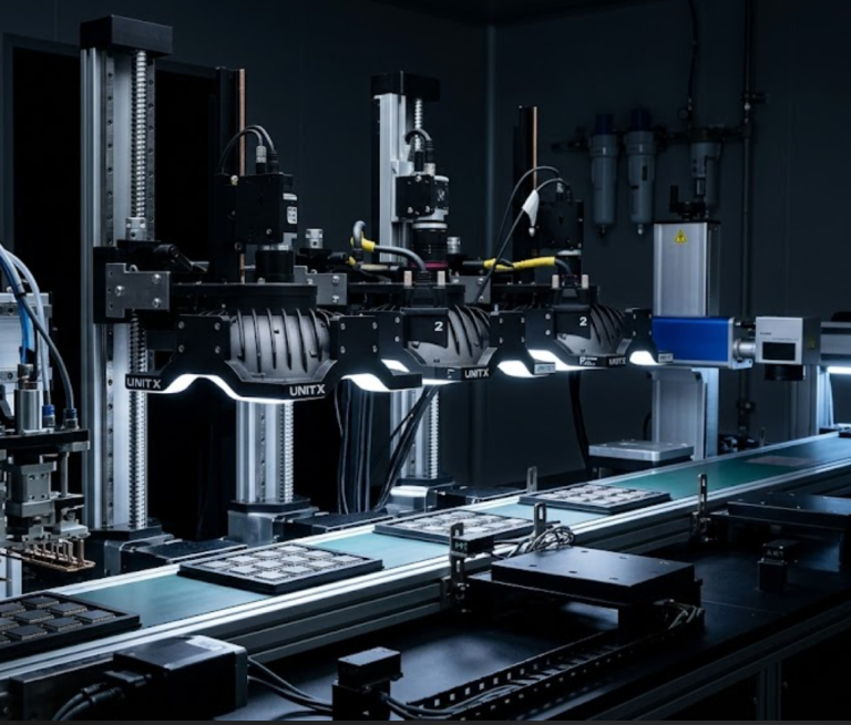
A 50 MP camera paired with fixed-angle, single-mode lighting will systematically miss surface scratches that only become visible under oblique illumination, or coating defects that require dark-field illumination to render as contrast. Software-defined lighting — systems that cycle through dozens of lighting configurations per second and composite the results — solves this problem.
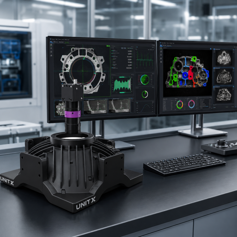
OptiX, UnitX’s imaging system, cycles through 50 lighting modes per second across 32 software-defined channels, enabling consistent defect visualization independent of surface material or texture variation. This level of architectural detail separates systems that perform well in demos from those that hold up in production.
2D vs 2.5D vs 3D: Matching Architecture to Your Defect Geometry
Standard 2D imaging handles surface defects on flat parts effectively. 2.5D imaging adds shallow depth profiling, which is essential for detecting raised burrs, solder paste volume variation, and connector pin height deviations — defects that are invisible to a pure 2D system regardless of resolution.
Full 3D scanning adds volumetric measurement capability but introduces cycle time costs that make it unsuitable for most high-throughput, in-line inspection applications. The right choice depends on your specific defect geometry, not vendor positioning. For most semiconductor and PCBA applications, 2.5D imaging delivers the required resolution without the throughput penalty of full 3D scanning.
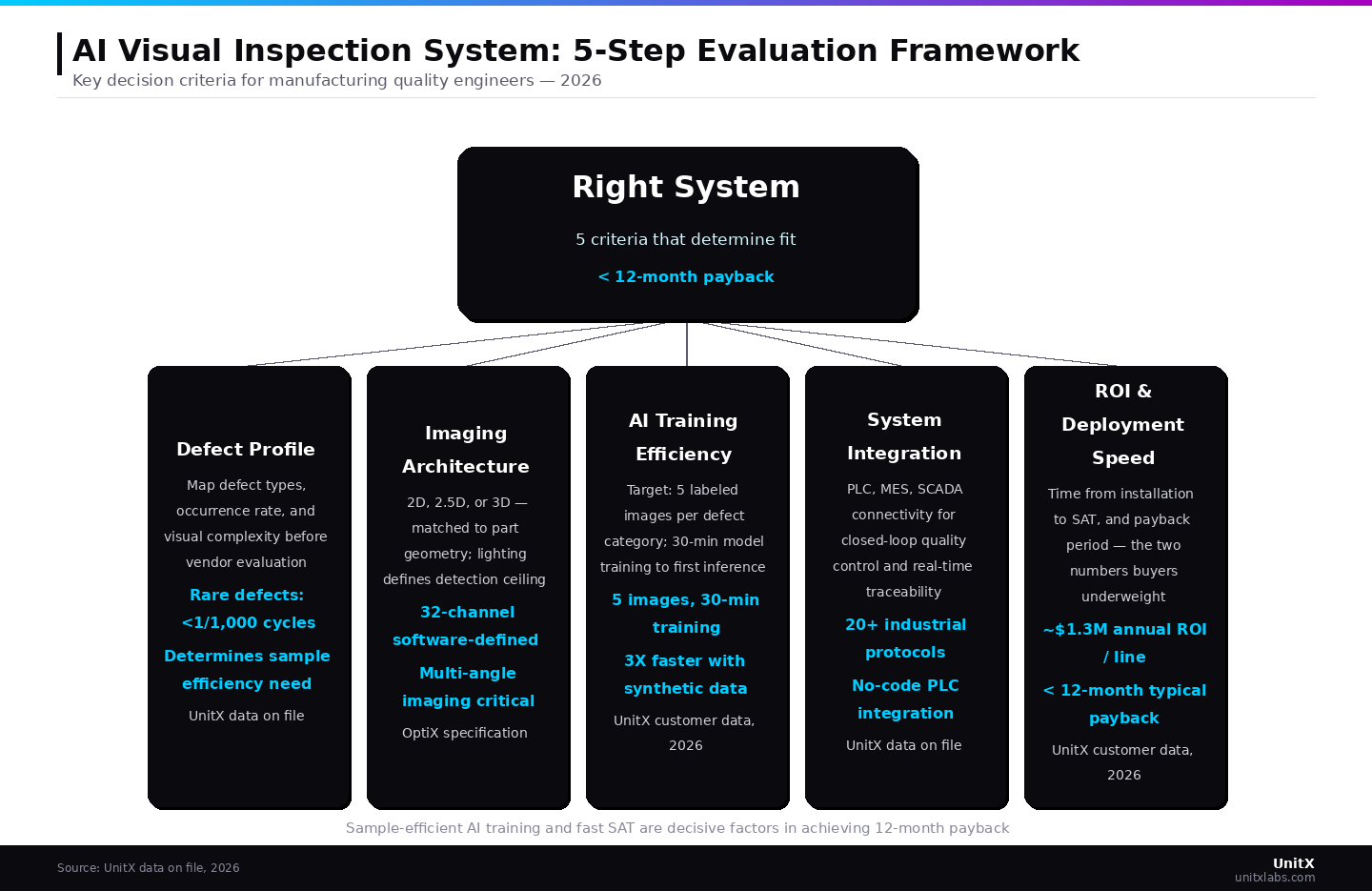
Sample-efficient AI training and fast SAT are decisive factors in achieving 12-month payback
Step 3: Assess AI Model Training Efficiency
The Five-Image Standard
Sample efficiency, the number of labeled defect images required to train a production-ready AI model — is the most consequential variable in your deployment timeline. Systems that require 500 to 5,000 labeled images per defect category (the requirement for most conventional deep learning approaches) make it impossible to deploy on rare-defect applications without months of pre-production data collection.
The benchmark: a sample-efficient AI inspection system should be capable of training an effective model from 5 labeled images per defect category, with initial deployment achievable within 30 minutes of labeling completion. According to UnitX’s production deployment data, combining sample-efficient AI with synthetic defect generation (using as few as 3 real samples) accelerates deployment by up to 3X and enables end-to-end site acceptance testing within 7 days.
Eight Detection Task Types: What Your System Must Handle
A complete AI visual inspection system should support eight fundamental detection task types: detection (defect presence), classification (defect type), counting (feature quantity), threshold (severity grading), localization (spatial position), measurement (dimensional), depth (Z-axis profiling), and barcode reading.
Systems optimized only for detection and classification — the most common configuration — may require engineering rework if your application later requires dimensional measurement or severity grading. Evaluating this capability upfront helps avoid costly platform changes 18 months post-deployment.
Explore the full UnitX product suite to see how OptiX, CorteX, and FleX-Gen address all eight detection task types within a single integrated platform.
Step 4: Integration — MES, PLC, and Traceability
An AI inspection system that delivers only a pass/fail signal, without pushing defect images, classification data, and trend metrics into your Manufacturing Execution System (MES) in real time, is a detection tool, not a full quality control system.
Closed-loop integration — where the AI system triggers PLC-level actions (reject mechanisms, conveyor stops, operator alerts) and writes traceability data to the MES — is what converts detection accuracy into measurable scrap and rework reduction.
Evaluate vendors on three criteria: the number of supported industrial protocols (20+ is typical for production-grade systems), whether PLC integration is no-code or requires custom programming, and whether MES data exchange uses open APIs or proprietary middleware. According to the 2025 Visual AI in Manufacturing landscape report, model explainability and integration complexity remain the top challenges cited by factory AI deployment teams.
Step 5: ROI and Deployment Timeline — The Numbers That Actually Matter
Site Acceptance Testing: What “Days to SAT” Measures
Site Acceptance Testing (SAT) marks the point at which the system is formally accepted as production-ready. The cost of delayed SAT is not just vendor fees — it includes lost production time due to continued reliance on manual inspection during qualification.
AI inspection systems designed for rapid deployment should target 5 days from installation to SAT. Systems requiring 6–12 week pilot phases introduce hidden costs that are often not reflected in RFQ comparisons.
ROI Benchmarks to Apply
Establishing a quantified ROI baseline before vendor selection provides a strong negotiating anchor and prevents unchallenged vendor claims. Based on UnitX production deployments: approximately $1.3M in annual ROI per production line (automotive Tier 1 average), payback periods under 12 months for high-variation defect inspection, approximately 3% scrap reduction, and up to 9X reduction in defect escapes compared to manual or rule-based inspection (UnitX customer data, 2026).
Manual inspection provides a useful baseline: it averages around 80% detection accuracy at best (Sandia National Laboratories, 2018), with performance degrading by 20–30% after just one hour of continuous monitoring. Any AI inspection system that cannot consistently exceed 99% detection accuracy for your specific defect profile represents a failed deployment.
Five Red Flags in AI Inspection Vendor Evaluations
Beyond the five evaluation steps above, watch for these patterns during vendor engagement.
First, vendors who present accuracy numbers without specifying the test conditions (part type, defect category, false rejection rate) are providing meaningless statistics — 99% accuracy on easy defects at high false rejection rates is not a useful benchmark.
Second, systems that require ML engineers to retrain models when production conditions change are not designed for factory-floor operation by quality teams.
Third, lighting architecture presented as a commodity rather than a differentiator should be a disqualifying signal for surface defect applications.
Fourth, ROI calculations that exclude data collection time, labeling effort, and MES integration costs systematically understate total cost of ownership.
Fifth, vendors who cannot provide documented SAT case studies with time-to-deployment data are presenting estimated rather than validated performance.
Book a demo to review documented UnitX deployment timelines for your specific part types and defect categories.
Frequently Asked Questions
How long does it realistically take to deploy an AI visual inspection system?
For a production-grade deployment using a sample-efficient AI platform, the timeline from installation to SAT should be 5–7 days for a single-line deployment with a defined defect profile. More complex applications — such as multiple defect categories, high-mix parts, or novel surface materials — may require 2–4 weeks.
Systems that require 3–6 month pilot phases typically indicate either a data collection bottleneck (insufficient sample efficiency) or integration complexity that should have been scoped prior to purchase. See UnitX case studies for documented SAT timelines across automotive, battery, and connector applications.
What is a reasonable false rejection rate target for AI visual inspection?
False rejection rate (FR) measures the proportion of acceptable parts incorrectly flagged as defective — the “overkill” rate that drives up scrap costs. A production-ready AI inspection system should achieve FR ≤ 1% for well-defined defect categories and FR ≤ 5% on high-variance cosmetic defects where acceptable and unacceptable conditions are inherently subjective.
Systems targeting FR = 0% across all categories are typically trading false rejection for false acceptance. A zero false rejection rate is not meaningful if it results in nonzero false acceptance—FA = 0% should remain the target for defect escapes.
Do I need a 3D inspection system or will 2D/2.5D suffice?
Full 3D scanning is required only when defect geometry is inherently volumetric — such as solder ball voiding, connector pin height variation beyond tolerance, or detailed surface profile measurement.
For most surface defect categories (scratches, dents, contamination, coating defects), 2.5D imaging, which combines surface texture capture with shallow depth profiling, provides the necessary detection performance without the cycle time penalty of full 3D scanning. Evaluate this based on your specific defect geometry and cycle time requirements, not vendor positioning.