Introduction: The Film That Protects the Chip
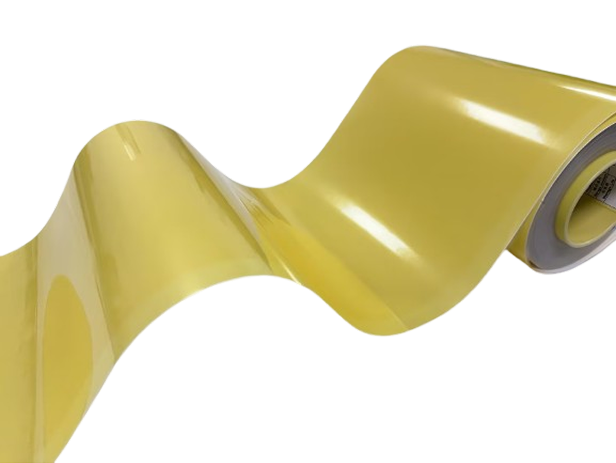
In semiconductor manufacturing, Wafer Film (often used for dicing, back-grinding, or photolithography) plays a critical protective role. It is the barrier between a delicate silicon wafer and the harsh manufacturing environment.
If this film has a defect—a tiny “black spot,” a bubble of “gel,” or a microscopic “pinhole”—it can translate into a disaster on the wafer itself. During etching or dicing, these film defects can cause pattern failures, leading to the scrapping of high-value chips.
Traditionally, this film was inspected manually using microscopes. But relying on humans to find micron-scale dots on a yellow transparent film is inefficient. Standards vary from person to person, miss rates are high, and false rejections waste expensive material.
The Challenge: High Value, Low Contrast
The project goal was to implement a reliable automated inspection method for these high-value, low-yield products.
The Defect Landscape:
The system needed to detect subtle anomalies that are often translucent or low-contrast against the yellow film:
- Contamination Hazards: Micro-particulates, black spots, stray fibers, and embedded impurities that threaten cleanroom standards.
- Process Flaws: Gel accumulation (bubbles) and panel patterns (surface marks) that can directly distort downstream photolithography or etching processes.

Wafer film requires flawless surface integrity to prevent etching errors on the silicon wafer.
The Solution: Automated AI Visual Inspection
UnitX deployed a high-precision automated visual inspection cell engineered to flawlessly inspect the reflective wafer film, effectively acting as an automated, high-speed “Digital Microscope.”

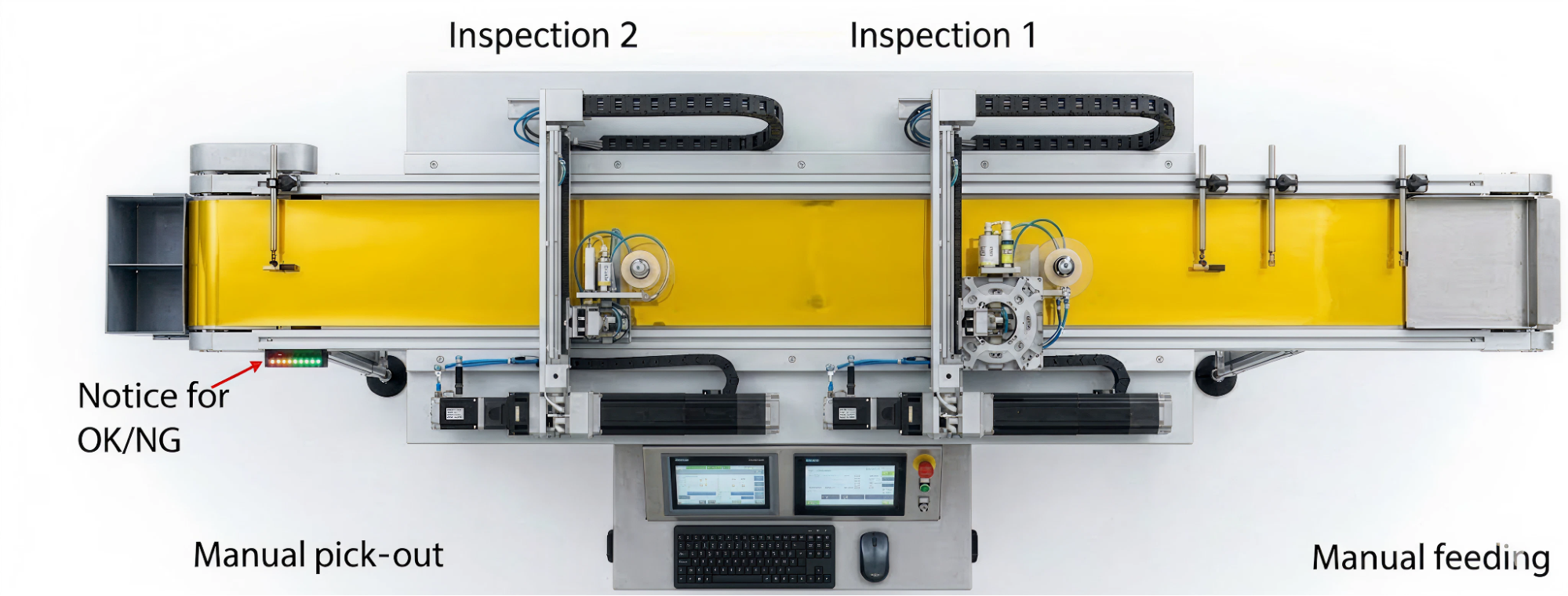
The UnitX system utilizes a lead-screw drive to move the camera for precise scanning of the film.
System Architecture:
- Precision Linear Motion: A highly stable lead screw module drives a single UnitX OptiX visual inspection system across the film, ensuring distortion-free, high-resolution imaging without mechanical vibration.
- Advanced Coaxial Optics: Equipped with a specialized parallel coaxial light source, the OptiX system overcomes the reflective, low-contrast surface of the film to cleanly illuminate surface anomalies like gel bubbles, panel marks, and microscopic fibers.
- Connected Traceability (MES): The CorteX AI system links all inspection data directly to the specific material roll number via the PLC. Results are uploaded instantly to the factory’s Manufacturing Execution System (MES), guaranteeing end-to-end traceability for the fab.
- Streamlined Workflow: Seamlessly integrating manual feeding and pick-out stations, the AI accurately flags defects on a digital dashboard, guiding operators with perfect, objective precision.
Results: Consistency in the Fab
The system brought objective standards to a previously subjective process.
1. Reliable Defect Capture
- False Acceptance Rate: ≤ 1%.
- The system acts as a robust filter, catching 99% of all defects. This reliability is crucial for preventing “killer defects” from reaching the wafer processing tools.
2. Cycle Time
- Cycle Time: 36 seconds per piece.
- While slower than consumer electronics inspection, this speed reflects the high-resolution, microscopic nature of the scan required for semiconductor materials.
3. Reduced Subjectivity
By replacing manual microscopic inspection, the manufacturer eliminated the “judgment calls” that led to inconsistent quality. Now, every roll of film is judged by the same rigorous AI standard.
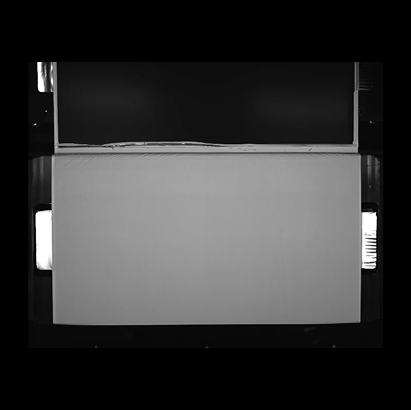
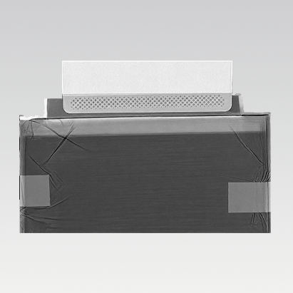
Defect Visualization
The images below show the challenge of detecting defects on textured surfaces.
- “Black Spot”: A clear contaminant.
- “Gel”: A subtle, translucent blob that changes the film’s thickness.
- “Panel Marks/Residue”: Surface scratches or glue.
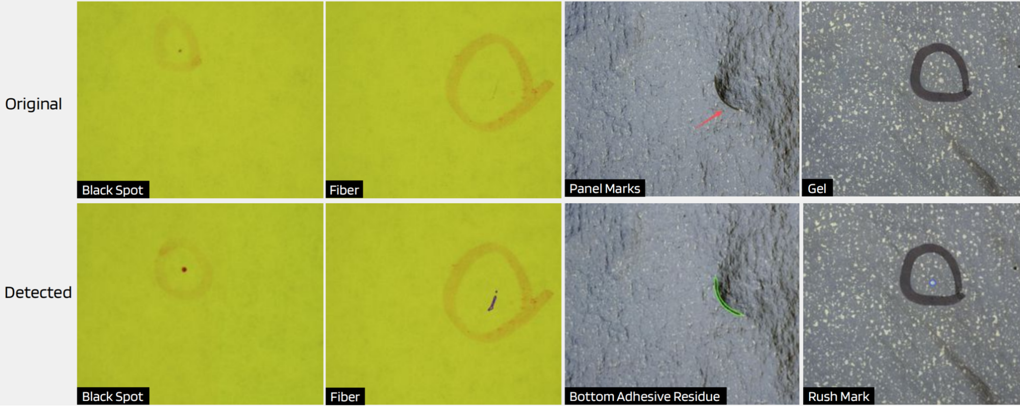
 UnitX AI identifies subtle defects like translucent gel and fibers on the wafer film.
Conclusion
In the semiconductor industry, yield is king. UnitX’s Wafer Film Inspection solution protects that yield by ensuring the materials you use are defect-free. By automating the microscopic search for impurities, we provide the assurance that your film will protect, not endanger, your wafers.
Secure your semiconductor materials.
Contact UnitX to discuss high-precision film inspection.