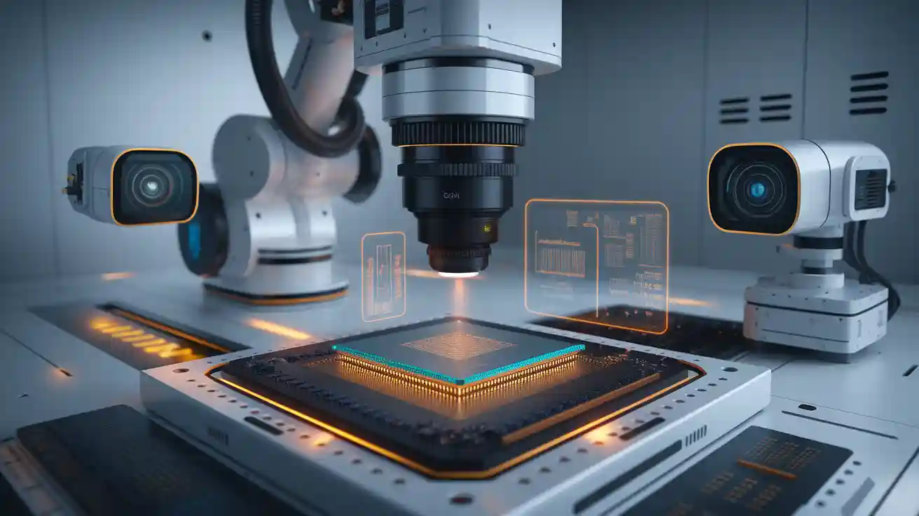
Semiconductors machine vision systems revolutionize how you approach manufacturing in the world of microelectronics. These systems utilize advanced imaging technology to inspect, measure, and monitor every stage of production. Their primary role is to ensure that each semiconductor meets strict quality standards.
Why are semiconductors machine vision systems so critical? Consider these key performance metrics:
-
Defect detection accuracy identifies microscopic flaws, ensuring only high-quality products move forward.
-
Yield optimization increases the number of usable chips per wafer, boosting profitability.
-
Process control efficiency allows real-time monitoring, improving consistency and quality.
With their precision and efficiency, semiconductors machine vision systems form the backbone of a reliable manufacturing system.
Key Takeaways
-
Semiconductor vision systems check products automatically, making them very accurate and reducing mistakes.
-
These systems find over 99% of defects, cutting waste and improving product quality.
-
Adding AI and machine learning helps these systems find problems better and handle new tasks.
-
Watching and analyzing in real-time makes production faster and lowers costs.
-
Using this technology helps companies stay ahead and grow in the semiconductor industry.
What Are Semiconductor Machine Vision Systems?
Definition and purpose
Semiconductor machine vision systems are advanced tools that use cameras, sensors, and software to inspect and analyze semiconductor components during manufacturing. These systems automate tasks like defect detection, precision measurement, and quality control, ensuring that every product meets strict standards.
You’ll find these systems essential in semiconductor manufacturing because they improve accuracy and efficiency. By automating inspection processes, they eliminate human error and speed up production. Semiconductor manufacturers were among the first to adopt this technology, accounting for nearly half of all machine vision applications. Over time, the technology has evolved, becoming more accessible and cost-effective for various industries.
Machine vision systems serve multiple purposes. They confirm the presence of electronic components on circuit boards, measure distances and areas with precision, and guide robots in assembling parts. They also extract text from images using optical character recognition and analyze barcode information. These functions make them indispensable in modern manufacturing environments.
Key features and capabilities
Semiconductor machine vision systems offer several features that enhance their performance. Cameras and sensors convert light into electric signals, enabling the system to process images. Area scan cameras capture entire images in one frame, making them ideal for uniform objects. Line scan cameras build images pixel by pixel, which works well for irregular or moving items. Sensitivity and resolution are critical specifications, allowing the system to operate in low light and differentiate between objects.
High-speed cameras play a vital role in semiconductor manufacturing. They quickly detect and locate defects in chips, improving the yield of non-defective products. Real-time processing capabilities ensure fast responses, which are crucial for timely interventions during production. Advanced object recognition allows the system to identify obstacles or flaws with precision, ensuring consistent quality.
Statistical data highlights the effectiveness of these systems. They achieve over 99% accuracy in detecting defects, reducing false positives significantly. Manufacturers report a 25% reduction in downtime due to early defect detection, which lowers operational costs by minimizing waste and rework rates.
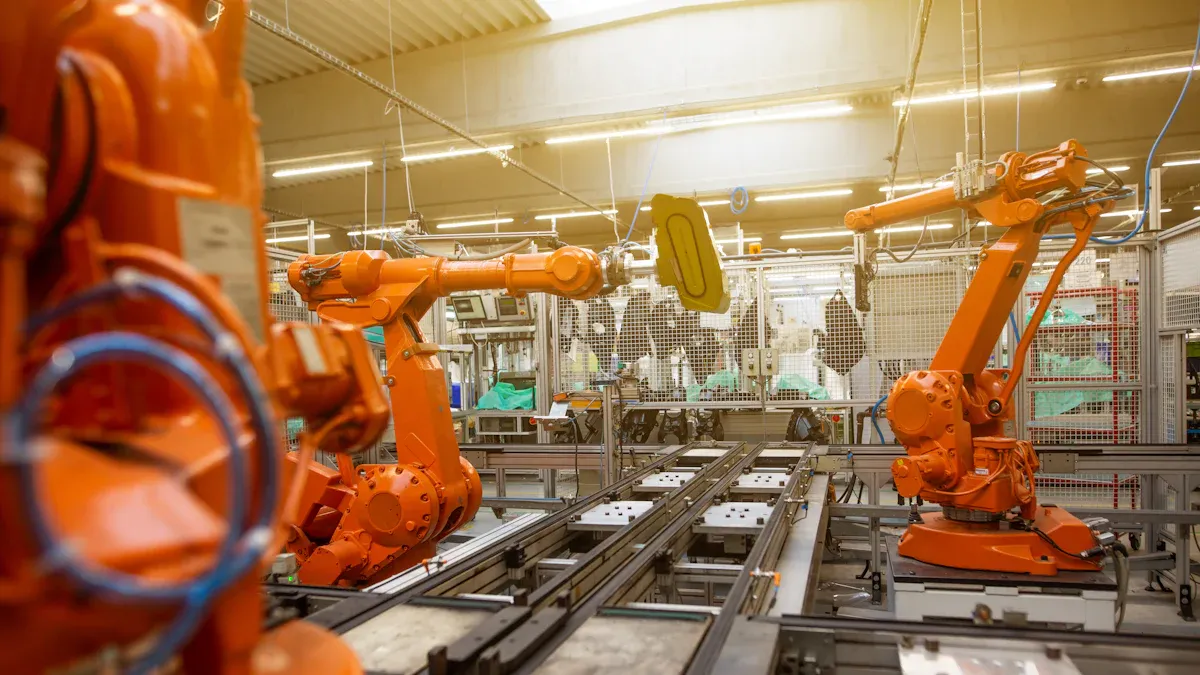
The versatility of machine vision systems extends beyond semiconductors. They are used in industries like automotive and electronics for tasks such as assembly, inspection, and quality control. Their ability to automate complex processes makes them a cornerstone of modern manufacturing.
How Do Semiconductor Machine Vision Systems Work?
Working process overview
Semiconductor machine vision systems operate by capturing and analyzing images of semiconductor components during manufacturing. The process begins with a sensor detecting light reflected from the object. This light is converted into an image, which the system processes to identify defects, measure dimensions, or verify alignment. Advanced image processing algorithms enhance the clarity of the captured image, making it easier to detect even microscopic flaws.
You can think of this system as a highly skilled inspector working at lightning speed. It examines every detail of a semiconductor wafer or chip, ensuring it meets strict quality standards. The system performs these tasks in real-time, allowing manufacturers to address issues immediately and maintain production efficiency.
Components of machine vision systems
A typical machine vision system consists of several key components. The sensor is the heart of the system, capturing light and converting it into an image. High-resolution cameras work alongside the sensor to ensure the image is detailed enough for analysis. Lighting systems illuminate the object, highlighting features that need inspection.
Processing units analyze the captured image using algorithms designed for specific tasks. These units rely on software to identify patterns, measure dimensions, and detect defects. The system also includes output devices that communicate results to operators or other machines in the production line.
Each component plays a vital role in ensuring the system functions effectively. For example, a high-quality sensor improves image clarity, while advanced software enhances the accuracy of defect detection.
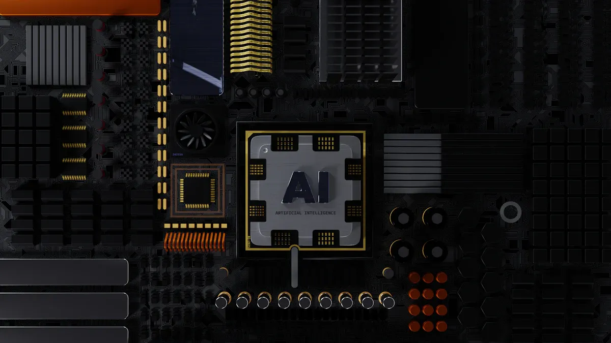
Role of AI and machine learning
AI and machine learning have transformed semiconductor machine vision systems. These technologies enable the system to learn from data and improve its performance over time. For instance, machine learning algorithms analyze patterns in images to identify defects more accurately. AI enhances the system’s ability to adapt to new challenges, such as detecting previously unseen flaws.
Here’s how AI and machine learning contribute to different areas of semiconductor manufacturing:
|
Application Area |
Contribution Description |
Example Company |
|---|---|---|
|
Electrochemical Deposition (ECD) |
Optimizes deposition rates and uniformity, identifies defects in real-time. |
GlobalFoundries |
|
Wafer Edge Inspection |
Analyzes wafer edges for defects, predicts impact on yield. |
KLA |
|
Plasma Etching Process Control |
Monitors plasma characteristics, adjusts parameters for uniformity. |
TSMC |
|
Wafer Map Analysis |
Detects patterns in wafer maps, groups defects for targeted solutions. |
NVIDIA |
|
Wafer-Level Testing |
Optimizes test coverage, adapts protocols based on trends. |
Synopsys, Mentor Graphics |
|
Contamination Control |
Monitors environmental data, optimizes filtration systems. |
Applied Materials |
By integrating AI, you can achieve higher accuracy and efficiency in semiconductor manufacturing. These systems not only detect defects but also predict potential issues, enabling proactive solutions. This combination of machine vision and artificial intelligence ensures consistent quality and reduces production costs.
Types of Machine Vision Systems in Semiconductor Manufacturing
2D imaging systems
2D imaging systems are the most common type of machine vision systems used in semiconductor manufacturing. These systems capture flat, two-dimensional images of objects, making them ideal for inspecting surface-level features. You can rely on these systems for tasks like defect detection, alignment verification, and materials inspection. They are particularly effective in identifying scratches, cracks, or contamination on semiconductor wafers.
One of the key technologies in 2D imaging is e-beam technology. It uses a focused beam of electrons to create high-resolution images, which are essential for semiconductor metrology. For example, the HMI eScan 1000 system increases inspection speed by nine times compared to traditional methods. This system achieves sub-nanometer precision by compensating for physical imperfections through advanced computational models. Additionally, its reticle stage accelerates at close to 16g, while the wafer stage reaches 7g, ensuring high-speed operation.
2D imaging systems are highly efficient for industrial applications. They focus on specific hotspots during inspection, improving accuracy and reducing time. These systems are a cornerstone of smart camera-based vision systems, which are widely used in semiconductor manufacturing.
3D imaging systems
3D imaging systems take inspection to the next level by capturing depth information along with surface details. These systems create three-dimensional models of objects, allowing you to analyze complex structures. They are particularly useful for inspecting stacked semiconductor components, where depth and height measurements are critical.
You can use 3D imaging systems to measure the thickness of wafers, detect warping, and ensure proper alignment of layers. These systems are essential for advanced industrial processes, where precision and accuracy are non-negotiable. By providing a comprehensive view of the object, 3D imaging systems help you identify defects that might go unnoticed in 2D images.
Hyperspectral imaging systems
Hyperspectral imaging systems offer a unique approach to materials inspection by capturing images across multiple wavelengths. Unlike traditional cameras, which capture only red, green, and blue light, hyperspectral systems analyze a wide range of spectral bands. This capability allows you to detect subtle differences in materials that are invisible to the human eye.
For example, a hyperspectral video imaging system captures video at a resolution of 128×128 with 64 spectral bands at 4.3 frames per second. Its data throughput is 900 times greater than conventional imaging systems. Additionally, the average light throughput for HyperspecI-V1 is 71.8%, while HyperspecI-V2 achieves 74.8%. In comparison, common RGB cameras have a throughput of less than 30%, and mosaic multispectral cameras fall below 10%.
These systems are invaluable for industrial applications, especially in semiconductor manufacturing. They excel at detecting contamination, analyzing materials, and ensuring the quality of raw materials. By integrating hyperspectral imaging into your production line, you can achieve unparalleled accuracy in materials inspection.
Applications of Machine Vision Systems in Semiconductor Manufacturing
Defect detection and classification
Machine vision systems excel at identifying and classifying defects in semiconductor manufacturing. These systems use advanced object recognition algorithms to detect flaws such as scratches, cracks, and contamination on wafers and chips. By analyzing images captured during production, they ensure that defective components are removed before they progress further.
You benefit from automated defect detection because it processes thousands of items per minute. This speed allows you to maintain high production rates without compromising quality. Real-time analysis ensures that even microscopic flaws are identified, reducing the risk of defective products reaching customers.
Machine vision systems achieve over 99% accuracy in defect detection, making them a reliable tool for maintaining quality standards. Manufacturers report significant cost reductions due to lower scrap rates and fewer customer returns. These systems not only enhance profitability but also improve customer satisfaction by delivering consistent quality.
Quality control and assurance
Quality control is a critical aspect of semiconductor manufacturing, and machine vision systems play a pivotal role in ensuring it. These systems perform real-time dimensional checks to verify that components meet strict specifications. By integrating with quality management systems, they allow you to track defect rates and make data-driven decisions to improve processes.
Machine vision systems offer unparalleled accuracy in object detection, achieving rates as high as 98.5%. This precision ensures that every object inspected meets the required standards. Automated processes eliminate human error, providing consistent results and reducing variability in quality control.
Tip: Implementing machine vision systems in your production line can significantly reduce downtime. Early detection of defects allows you to address issues promptly, minimizing disruptions and maintaining efficiency.
The ability to monitor quality continuously helps you optimize manufacturing processes. By reducing waste and rework, these systems lower operational costs and improve overall productivity.
Precision measurement and alignment
Precision measurement and alignment are essential for producing high-quality semiconductors. Machine vision systems use advanced imaging techniques to measure dimensions and align components with exceptional accuracy. These systems analyze images to ensure that wafers, chips, and other objects are positioned correctly during manufacturing.
You can rely on machine vision systems to perform real-time dimensional checks, ensuring adherence to specifications. For example, they measure wafer thickness, detect warping, and verify the alignment of stacked layers. These tasks are crucial for maintaining the integrity of semiconductor components.
The integration of object recognition technology enhances the accuracy of these systems. By identifying patterns and features in images, they ensure that every object is inspected thoroughly. This capability reduces the risk of errors and improves the overall quality of the final product.
|
Metric |
Value |
|---|---|
|
Accuracy in defect detection |
Over 99% |
|
Accuracy in object detection |
98.5% |
Machine vision systems contribute to cost savings by minimizing waste and improving yield. Their ability to perform precise measurements and alignments ensures that every component meets the highest standards of quality.
Benefits of Machine Vision Systems in Semiconductor Manufacturing
Improved accuracy and precision
Machine vision systems bring unparalleled accuracy to semiconductor manufacturing. These systems inspect wafers and chips at a microscopic level, identifying even the smallest defects. By automating this process, you eliminate human error and ensure consistent quality. For example, machine vision systems achieve over 99% accuracy in defect detection, making them a reliable tool for maintaining high standards.
The precision of these systems also extends to measurements. They analyze dimensions and align components with exceptional accuracy, ensuring that every semiconductor meets strict specifications. This level of precision reduces the risk of defective products and enhances customer satisfaction.
Enhanced efficiency and productivity
Machine vision systems significantly improve the efficiency of semiconductor manufacturing. They process thousands of components per minute, allowing you to maintain high production rates without compromising quality. Real-time analysis ensures that defects are detected and addressed immediately, minimizing downtime.
The impact of these systems on productivity is evident in the industry’s growth. In 2024, the market value of machine vision systems is projected to reach $611 billion, with a growth rate of 16%. By 2025, this value is expected to rise to $687 billion, reflecting a 12.5% growth rate. These figures highlight the increasing reliance on machine vision systems for efficient manufacturing.
|
Year |
Market Value (in billion USD) |
Growth Rate (%) |
|---|---|---|
|
2024 |
611 |
16 |
|
2025 |
687 |
12.5 |
Cost reduction through automation
Automation is a key benefit of machine vision systems. By automating inspection and quality control processes, you reduce labor costs and minimize waste. These systems ensure consistent product quality, which lowers the risk of customer returns and warranty claims.
Machine vision systems also improve manufacturing efficiency by reducing defects. This leads to lower scrap rates and higher yields, ultimately saving you money. Additionally, the ability to detect and address issues in real-time prevents costly production delays.
Note: Machine vision systems not only enhance efficiency but also contribute to long-term cost savings. Their ability to automate complex tasks makes them an invaluable asset in semiconductor manufacturing.
Machine Vision vs. Computer Vision in Semiconductor Manufacturing
Differences in scope and functionality
Machine vision and computer vision share similarities but differ in scope and functionality. Machine vision focuses on industrial applications, particularly in semiconductor manufacturing. It uses cameras, sensors, and software to inspect and analyze components during production. You can rely on machine vision systems to automate tasks like defect detection, precision measurement, and alignment. These systems operate in real-time, ensuring efficiency and accuracy in manufacturing processes.
Computer vision, on the other hand, has a broader scope. It aims to replicate human vision by enabling computers to interpret and understand visual data. While machine vision is task-specific, computer vision applies to various fields, including healthcare, security, and entertainment. For example, computer vision powers facial recognition systems and autonomous vehicles.
The table below highlights the approaches used in semiconductor manufacturing:
|
Approach Type |
Description |
|---|---|
|
Conventional Baseline |
Utilizes image processing techniques such as projection-based and filter-based methods. |
|
Machine Learning (ML) |
Employs advanced algorithms for improved detection and classification rates in fault inspection. |
|
Deep Learning (DL) |
Leverages neural networks for enhanced performance in identifying defects in semiconductor products. |
Machine vision systems often integrate machine learning and deep learning to enhance their capabilities. These technologies improve defect detection and classification, making machine vision indispensable in semiconductor manufacturing.
Unique roles in semiconductor manufacturing
Machine vision plays a specialized role in semiconductor manufacturing. It ensures that every component meets strict quality standards. You can use machine vision systems to inspect wafers, detect defects, and measure dimensions with high precision. These systems excel at automating repetitive tasks, reducing human error, and increasing production efficiency.
Computer vision contributes to semiconductor manufacturing by enabling advanced analytics and decision-making. For instance, it helps analyze large datasets to identify patterns and trends. This capability supports process optimization and predictive maintenance. However, computer vision lacks the real-time processing and task-specific focus of machine vision systems.
In semiconductor manufacturing, machine vision systems dominate due to their speed, accuracy, and reliability. They are tailored to meet the industry’s unique demands, making them a cornerstone of modern production lines.
Semiconductor machine vision systems play a vital role in modern manufacturing. They ensure precision, improve efficiency, and maintain high-quality standards. By automating complex tasks, these systems help you reduce errors and optimize production processes.
Key Insight: Machine vision systems have revolutionized semiconductor manufacturing by enabling real-time defect detection and advanced quality control.
Looking ahead, the integration of AI and machine learning will unlock even greater potential. You can expect smarter, faster, and more adaptive systems that will redefine the future of semiconductor production. Embracing this technology positions you at the forefront of innovation.
FAQ
What is the difference between 2D and 3D imaging systems in semiconductor manufacturing?
2D imaging systems capture flat images for surface-level inspections. 3D imaging systems create depth models, allowing you to analyze complex structures like stacked layers. Use 2D for scratches and contamination; rely on 3D for thickness and alignment checks.
How does AI improve machine vision systems?
AI enables systems to learn from data and adapt to new challenges. It enhances defect detection, predicts issues, and optimizes processes. You benefit from smarter, faster, and more accurate inspections.
Can machine vision systems reduce production costs?
Yes, automation lowers labor costs and minimizes waste. Early defect detection reduces scrap rates and prevents delays. These systems improve efficiency, saving you money in the long run.
Are hyperspectral imaging systems necessary for semiconductor manufacturing?
Hyperspectral systems analyze materials across multiple wavelengths. They detect subtle differences invisible to standard cameras. Use them for contamination control and raw material inspections to ensure high-quality production.
What industries use machine vision systems besides semiconductors?
Machine vision systems are widely used in automotive, electronics, and pharmaceuticals. They perform tasks like assembly, inspection, and quality control. Their versatility makes them essential across industries.
See Also
Understanding Electronics in Machine Vision Systems Today
An In-Depth Overview of Machine Vision in Automation
How to Properly Position Equipment in Vision Systems
Exploring Image Processing Techniques in Vision Systems
Comparing Firmware Machine Vision With Conventional Systems