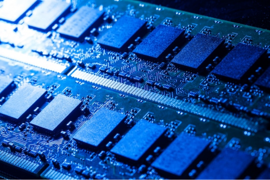
Quality inspection manufacturing of semiconductors ensures that every product meets the highest standards for performance and reliability. You rely on this process to detect defects early, safeguard product functionality, and maintain trust in the semiconductor industry. The intricate nature of semiconductor manufacturing demands unmatched precision. With billions of transistors packed into nanometer-scale designs, even the smallest imperfection can compromise quality. Advanced inspection techniques, combined with rigorous quality control, play a pivotal role in delivering reliable semiconductors that power modern technology.
The Basics of Quality Inspection Manufacturing of Semiconductors
Quality inspection forms the backbone of semiconductor manufacturing. You ensure that every chip meets strict performance and reliability standards by implementing thorough inspection processes. This step is essential because semiconductors operate at the heart of modern technology, powering devices from smartphones to medical equipment.
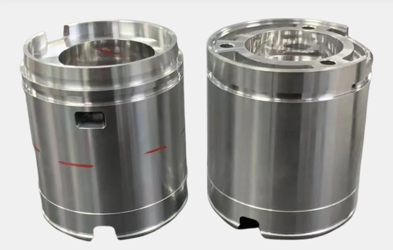
The manufacturing process involves hundreds of intricate steps, each requiring precision. Even the smallest defect can compromise the functionality of a semiconductor. Physical inspections focus on identifying surface-level issues like contamination, deformities, or incorrect dimensions. Functional inspections verify that each chip performs as intended. Together, these methods help you maintain the high-quality standards expected in the industry.
Advanced tools and techniques have revolutionized quality inspection. High-resolution cameras combined with machine learning algorithms detect microscopic flaws that traditional methods might miss. Automated systems analyze wafers in real time, ensuring consistency and reducing human error. These innovations allow you to meet the growing demand for semiconductors without sacrificing quality.
The importance of quality inspection extends beyond production. It ensures compliance with stringent regulatory standards, especially for industries like aerospace and healthcare. By adhering to these standards, you protect your reputation and build trust with customers. Moreover, effective inspection processes reduce waste, optimize resources, and improve cost efficiency.
In today’s fast-paced world, digitalization has become a game-changer. Real-time data analytics and predictive maintenance tools enhance the accuracy of inspections. Digital twins, virtual replicas of physical systems, allow you to simulate and address potential issues before they occur. These advancements not only improve quality but also streamline the entire manufacturing process.
By prioritizing quality inspection, you contribute to a sustainable and ethical semiconductor industry. Transparent processes and responsible practices ensure that your products meet the highest standards while minimizing environmental impact. This commitment to excellence positions you as a leader in the ever-evolving world of semiconductor manufacturing.
Methods and Tools for Semiconductor Testing
The semiconductor testing process is a cornerstone of ensuring the reliability and functionality of modern electronic devices. By employing advanced tools and techniques, you can identify defects early and maintain high-quality standards throughout production. This section explores the common inspection techniques and cutting-edge technologies that drive the semiconductor testing process.
Common Inspection Techniques
Visual inspection for surface-level defects
Visual inspection serves as the first line of defense in semiconductor testing. You can detect surface-level defects such as scratches, contamination, or pattern misalignments by using high-resolution cameras and sophisticated imaging techniques. This method ensures that wafers and dies meet the required physical standards before moving to more advanced testing stages.
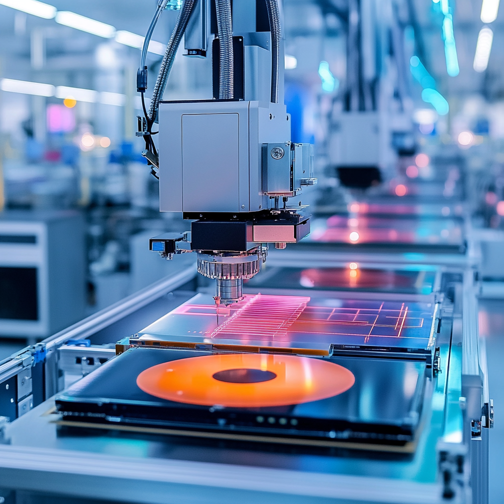
Automated optical inspection (AOI) for detecting microscopic flaws
Automated optical inspection (AOI) revolutionizes the semiconductor testing process by identifying microscopic flaws that are invisible to the naked eye. High-speed cameras and advanced lighting systems work together to scan wafers and dies for imperfections. AOI systems analyze images in real time, allowing you to maintain consistency and reduce human error during quality control practices.
X-ray inspection for internal structural analysis
X-ray inspection provides a deeper look into the internal structures of semiconductors. This technique is essential for detecting hidden defects, such as voids or cracks, that could compromise the reliability of the final product. By using X-ray inspection, you can ensure that the internal components of wafers and packages meet stringent quality control standards.
Advanced Technologies in Semiconductor Testing
The role of AI and machine learning in defect detection
Artificial intelligence (AI) and machine learning have transformed semiconductor testing. These technologies analyze vast amounts of data to identify patterns and predict potential defects. By integrating AI into your testing process, you can enhance accuracy and streamline defect detection, ensuring that only high-quality devices reach the market.
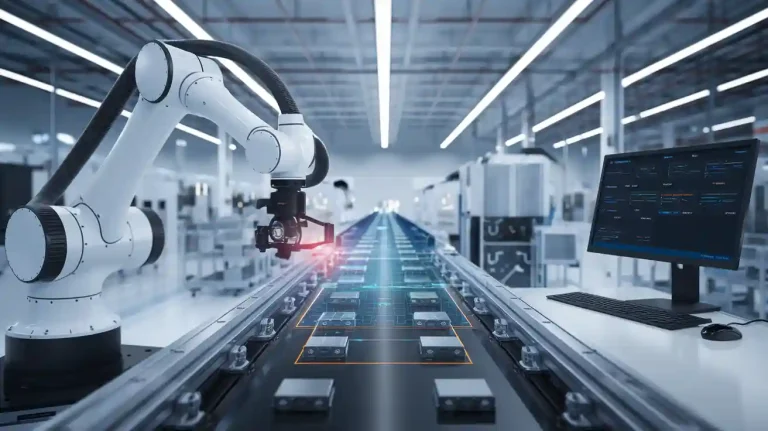
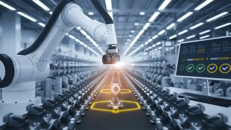
Robotics for precision and consistency in inspection
Robotics plays a crucial role in maintaining precision and consistency during semiconductor testing. Automated systems handle delicate wafers and dies with unparalleled accuracy, reducing the risk of damage. Robotics also accelerates the testing process, enabling you to meet the growing demand for semiconductors without compromising quality.
Data analytics for predictive quality control
Data analytics empowers you to take a proactive approach to quality control. By analyzing historical and real-time data, you can predict potential issues and implement corrective measures before defects occur. Predictive quality control not only improves the efficiency of the semiconductor testing process but also minimizes waste and optimizes resource utilization.
The Role of Digitalization in Quality Inspection Manufacturing of Semiconductors

Digitalization has transformed the way you approach quality inspection in semiconductor manufacturing. By integrating advanced technologies, you can achieve higher precision, faster processes, and improved outcomes. Traditional inspection methods often rely on manual efforts or basic automation, which can limit accuracy and efficiency. Digitalized systems, however, bring a new level of sophistication to the inspection process.
One of the key advantages of digitalization lies in its ability to automate defect detection. By combining digital holography with image processing and machine learning algorithms, you can identify and classify defects with remarkable speed and accuracy. This approach not only reduces the time spent on inspections but also enhances productivity and manufacturing yields. For example, automated systems can detect microscopic anomalies that might go unnoticed with traditional methods, ensuring consistent quality across all semiconductor products.
Another benefit of digitalization is its seamless integration with existing systems. Digital solutions act as a software layer on top of your current hardware, utilizing images from existing cameras. This eliminates the need for costly hardware upgrades while improving inspection processes. You can enhance decision-making and streamline operations without overhauling your entire setup.
Real-time data analytics plays a crucial role in digitalized quality inspection. By analyzing data as it is generated, you can make immediate adjustments to the manufacturing process. This proactive approach helps you prevent defects before they occur, reducing waste and optimizing resource utilization. Predictive maintenance tools, powered by digital twins, allow you to simulate potential issues and address them early, further enhancing efficiency.
Digitalization also ensures compliance with stringent industry standards. Automated systems generate detailed reports and audit trails, simplifying regulatory submissions. This transparency builds trust with customers and positions you as a reliable leader in the semiconductor industry.
By embracing digitalization, you not only improve the quality of your products but also future-proof your manufacturing processes. The integration of cutting-edge technologies ensures that you stay ahead in an increasingly competitive market. Digitalized quality inspection is not just an upgrade; it is a necessity for achieving excellence in semiconductor manufacturing.
Best Practices for Simplifying Semiconductor Testing
Simplifying semiconductor testing requires a strategic approach that balances efficiency with precision. By adopting best practices, you can streamline processes, reduce errors, and ensure consistent quality. Here are some actionable steps to enhance your testing workflow:
1. Standardize Testing Procedures
Establishing clear and standardized testing protocols ensures consistency across all stages of semiconductor production. Document each step of the testing process, from initial inspections to final validations. This approach minimizes variability and helps you maintain high-quality standards.
Tip: Use checklists and templates to guide your team through each testing phase. This reduces the likelihood of oversight and ensures uniformity.
2. Leverage Automation for Efficiency
Automation plays a critical role in simplifying semiconductor testing. Automated systems handle repetitive tasks with speed and accuracy, freeing up your team to focus on more complex challenges. For example, automated optical inspection (AOI) systems can quickly identify defects that might be missed during manual inspections.
-
Benefits of automation:
-
Faster testing cycles.
-
Reduced human error.
-
Improved scalability to meet growing demands.
-
3. Integrate Real-Time Data Analytics
Real-time data analytics enhances decision-making during the testing process. By analyzing data as it is generated, you can identify trends, predict potential issues, and implement corrective actions immediately. This proactive approach improves efficiency and reduces waste.
Example: Predictive analytics tools can flag anomalies in wafer production, allowing you to address problems before they escalate.
4. Train Your Team on Advanced Tools
Investing in training ensures your team can effectively use advanced testing tools and technologies. Familiarity with robotics, AI-driven systems, and data analytics platforms empowers your team to maximize the potential of these innovations.
Key Insight: A well-trained team not only improves testing accuracy but also boosts overall productivity.
5. Optimize Lab Layouts and Workflows
An optimized lab layout reduces bottlenecks and enhances workflow efficiency. Arrange equipment logically to minimize movement and ensure smooth transitions between testing stages. Modernizing your lab with ergonomic designs and advanced tools can significantly impact project timelines and costs.
Implementing small changes in lab organization can lead to substantial improvements in efficiency and output.
6. Prioritize Quality Assurance and Control Practices
Strong quality assurance and control practices form the foundation of effective semiconductor testing. Regularly review and update your testing protocols to align with industry standards. Incorporate feedback loops to continuously improve processes and outcomes.
Remember: Consistent quality assurance builds trust with customers and ensures compliance with regulatory requirements.
By following these best practices, you can simplify semiconductor testing while maintaining the highest standards of quality. These strategies not only improve efficiency but also position you as a leader in the competitive semiconductor industry.
Benefits of Effective Quality Inspection in Semiconductor Manufacturing
Effective quality inspection in semiconductor manufacturing delivers significant advantages that enhance your production processes and ensure the reliability of your products. By prioritizing quality assurance, you can achieve better outcomes across multiple aspects of your operations.
1. Improved Product Reliability
Quality assurance ensures that every semiconductor meets stringent standards for performance and reliability. By identifying and addressing defects early, you can prevent faulty products from entering the market. This proactive approach builds trust with your customers and strengthens your reputation in the semiconductor industry.
Fact: Reliable semiconductors power critical applications, from medical devices to aerospace systems, where failure is not an option.
2. Enhanced Product Quality
Thorough quality assurance processes help you maintain consistent product quality. Advanced inspection techniques, such as automated optical inspection and X-ray analysis, detect even the smallest imperfections. These methods ensure that your semiconductors meet the highest standards, reinforcing your commitment to excellence.
3. Cost Savings Through Waste Reduction
Effective quality inspection minimizes waste by catching defects before they escalate. By improving yield rates and reducing the number of defective products, you can optimize resource utilization and lower production costs. This efficiency translates into significant financial savings for your operations.
-
Key Benefits:
-
Reduced material waste.
-
Lower rework and repair costs.
-
Increased profitability.
-
4. Compliance with Industry Standards
Stringent regulatory standards govern the semiconductor industry, especially for applications in healthcare, automotive, and aerospace. Quality assurance processes ensure that your products comply with these regulations. Automated systems generate detailed reports, simplifying audits and regulatory submissions.
Insight: Compliance not only avoids penalties but also positions you as a reliable partner in the global market.
5. Increased Customer Satisfaction
High product quality and reliability lead to greater customer satisfaction. When your semiconductors consistently perform as expected, you build long-term relationships with clients. Satisfied customers are more likely to return for future business and recommend your products to others.
6. Competitive Advantage in the Market
By investing in quality assurance, you gain a competitive edge in the semiconductor industry. Superior product quality and reliability set you apart from competitors. This distinction helps you attract new customers and expand your market share.
7. Future-Proofing Your Manufacturing Processes
Advanced quality assurance techniques, such as digitalization and predictive analytics, prepare you for future challenges. These innovations enable you to adapt to evolving industry demands while maintaining high standards. By embracing these technologies, you ensure the long-term success of your manufacturing operations.
Example: Digital twins allow you to simulate potential issues and address them proactively, reducing downtime and improving efficiency.
Effective quality inspection is not just a process; it is a strategic investment in the success of your semiconductor manufacturing. By focusing on reliability, product quality, and compliance, you can achieve sustainable growth and establish yourself as a leader in the industry.
Quality inspection in semiconductor manufacturing plays a vital role in ensuring product reliability, reducing costs, and enhancing customer satisfaction. By adopting advanced tools, embracing digitalization, and training your team effectively, you can simplify the inspection process and achieve consistent results. Prioritizing quality inspection not only safeguards your reputation but also positions you as a leader in the competitive semiconductor industry.
For unparalleled accuracy and efficiency, consider UnitX’s vision system. Its AI-driven technology automates inspections, detects defects across all stages, and ensures the highest quality standards in semiconductor production.
FAQ
What is the importance of semiconductor inspection and metrology?
Semiconductor inspection and metrology are essential for maintaining the quality and reliability of semiconductor devices. By using advanced technologies and precise measurement techniques, you can detect defects early, optimize manufacturing processes, and improve product performance. These practices ensure that every semiconductor meets the high standards required for modern electronic applications.
What are the criteria for selecting semiconductor inspection equipment?
When choosing semiconductor inspection equipment, you should consider several factors. The diameter of the wafer, the specific manufacturing process, and the types of defects you aim to detect are critical. Selecting the right equipment helps you identify defective products early, reduce costs, and enhance the overall quality and reliability of your production.
Why is wafer and semiconductor inspection important during production?
Wafer and semiconductor inspection play a crucial role in ensuring the quality of integrated circuits and other electronic components. During production, this process helps you detect and analyze defects, scratches, or contamination that may arise. Addressing these issues promptly prevents performance failures and ensures a smooth production flow.
What is the role of quality control in the semiconductor industry?
Quality control serves as the foundation of the semiconductor industry. It ensures that your products meet strict standards for reliability and performance. By implementing robust quality control measures, you can reduce manufacturing costs, enhance product reliability, and maintain your reputation in the competitive semiconductor market.
Why is the integrity of data and measurements critical in semiconductor inspections?
Accurate data and measurements are vital in semiconductor inspections. Without reliable measurements, inspection tools become subjective and less effective. For example, calibrated digital microscopes ensure precise measurements at every magnification, providing you with consistent and traceable results. This accuracy is essential for maintaining high-quality standards.
How do advanced inspection systems improve yield and efficiency in semiconductor manufacturing?
Advanced inspection systems enhance yield and efficiency by identifying surface defects and addressing imperfections during production. These systems use cutting-edge technologies like high-resolution imaging and machine learning to detect flaws quickly. By integrating these tools, you can improve manufacturing throughput and ensure consistent product quality.
What is the role of inspection in the semiconductor wafer manufacturing process?
Inspection in wafer manufacturing ensures that each wafer meets the required specifications before moving to the next production stage. This process helps you identify defects, such as contamination or structural inconsistencies, that could compromise the final product. Regular inspections maintain the integrity of your manufacturing process and improve overall efficiency.
How does digitalization transform semiconductor quality inspection?
Digitalization revolutionizes quality inspection by automating defect detection and streamlining processes. With tools like real-time data analytics and predictive maintenance, you can address potential issues before they escalate. Digital twins allow you to simulate scenarios and optimize production, ensuring higher precision and faster results.
What are the benefits of using AI in semiconductor inspections?
AI enhances semiconductor inspections by analyzing large datasets to identify patterns and predict defects. By incorporating AI-driven systems, you can improve accuracy, reduce human error, and accelerate the inspection process. These advancements ensure that only high-quality semiconductors reach the market.
How can you simplify semiconductor testing while maintaining quality?
You can simplify semiconductor testing by standardizing procedures, leveraging automation, and integrating real-time data analytics. Training your team on advanced tools and optimizing workflows also contribute to efficiency. These strategies help you maintain high-quality standards while reducing complexity in the testing process.
See Also
An In-Depth Look at Machine Vision in Automation
UnitX OptiX: Revolutionizing the Inspection Process
The Impact of Generative AI on Manufacturing’s Future