Electronics
Electronics are used in critical applications, including medical devices, automotive systems, and aerospace. Ensuring the reliability and safety of these products is paramount to avoid failures that could lead to serious consequences, including loss of life.
Applications
UnitX automates inspection across all seminconductor manufacturing processes such as:
123
Semiconductors wafers are composed of individual layers, each undergoing a meticulous sequence of processes such as lithography, etching, ion implantation, and deposition. Each individual layer needs to be inspected for defects before the next layer is applied– if a defect is missed at this stage, it may only be caught at final testing or not at all.
UnitX detects wafer defects that, if undetected prior to layering, can compromise chip performance and lead to premature failure.
123
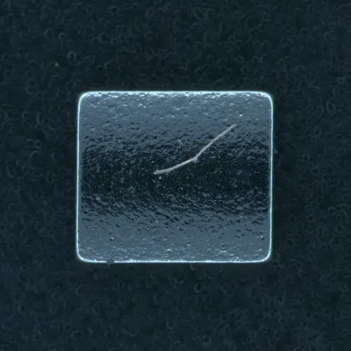
After they are processed, wafers undergo electrical testing to identify faulty circuits. Then the wafers cut into individual semiconductor devices or dies that can then be packaged into a final integrated circuit (IC). The goal of dicing is to separate the dies while minimizing damage to the wafer and ensuring the integrity of each die.
UnitX detects defective testing equipment that can lead to faulty electrical testing and impact die yields. UnitX also detects dicing defects that can ultimately lead to degraded performance and device failure. Its detection models are able to distinguish between normal marks on wafers and defects that may signal issues with the testing and dicing technologies themselves. And UnitX’s configurable threshold capabilities allowing users to specify which defects are within acceptable tolerances and which are not in order to minimize waste.
123
Dies are then packaged into a final integrated circuit (IC). First, dies are mounted onto a package and provided connections so it can be integrated into electronic devices. Thin wires are bonded to the chip and package to provide a path for signals and power to travel into and out of the chip. Then the chip and wire bonds are encapsulated in protective material to prevent damange.
UnitX detects defects throughout the packaging process, ranging from cosmetic problems to those that compromise an IC’s structural integrity and protection against the environment, which can result in catastrophic failure.
Solutions
(via integration with third party vision systems)
Rapid deployment of UnitX AI with existing systems. UnitX’s CorteX integrates with specialized semiconductor optical inspection equipment and X-Rays to detect and classify sub-micron wafer fabrication and advanced packaging defects
Advantages
UnitX’s unique advantages ultimately help semiconductor manufacturers ensure quality while improving yield:
Reduced cost
100% automated inline inspection replaces need for manual inspectors
Increased throughput
High-speed imaging & AI inference speeds that match cycle times
Reduced waste
Deployable across all stages of semiconductor manufacturing processes to identify defects early in the production process and provide rapid corrective action
Reduced escapes
Accurately detects defects that are highly variable and complex in shape, size, and presentation
Reduced overkill
Distinguishes functional defects from normal marks/patterns as part of manufacturing process. Adjustable thresholds to distinguish unacceptable defects from defects that are within tolerances
Introducing
UnitX
UnitX provides AI vision to help manufacturers automate inspection. Electronics manufacturers use UnitX solutions to detect defects across many manufacturing processes such as battery, semiconductor, conductor, and PCBA applications.
Electronics Application Examples
To learn more about how UnitX can automate inspection for you, please contact us here